SPI Stream Configuration using the TI ADS833x Example
Overview
The purpose of this paper is to take an in-depth look at how to choose the NI-845x SPI Stream Configuration parameters for the TI ADS833x EVM example from the TI ADS833x datasheet (1). Please use this page to follow along with the shipped example and apply the concepts in other applications. The example can be located at: C:\Program Files (x86)\National Instruments\LabVIEW 2021\examples\ni845x\845xEx.llb and is installed with the NI-845x Driver.
Contents
- Introduction
- TI ADS833x Datasheet Timing
- SPI Stream Configuration Property Node
- Configuring CONV, DRDY, and CS
- Determining Clock Phase and Polarity
- Determining Necessary Timing Parameters
- Determining Number of Samples, Number of Bits Per Sample, and MOSI Data
- Resulting Waveform
- Resources
Introduction
The purpose of this paper is to take an in-depth look at how to choose the NI-845x SPI Stream Configuration parameters for the TI ADS833x EVM example from the TI ADS833x datasheet (1). The TI ADS833x supports several modes of operation, which are summarized in Table 1 (page 22) of the datasheet. For this example, we want to sample a single channel continuously. The datasheet specifies below Table 1 that this is achieved with Manual Channel select in Auto-Trigger mode. For this example, we use the EVM’s onboard 5 V regulator described on page 5 of the TI ADS833x EVM User Guide(2) as a power supply. The master device is the NI USB-8452. Note that the SPI Stream API is not available for the NI-8451.
TI ADS833x Datasheet Timing
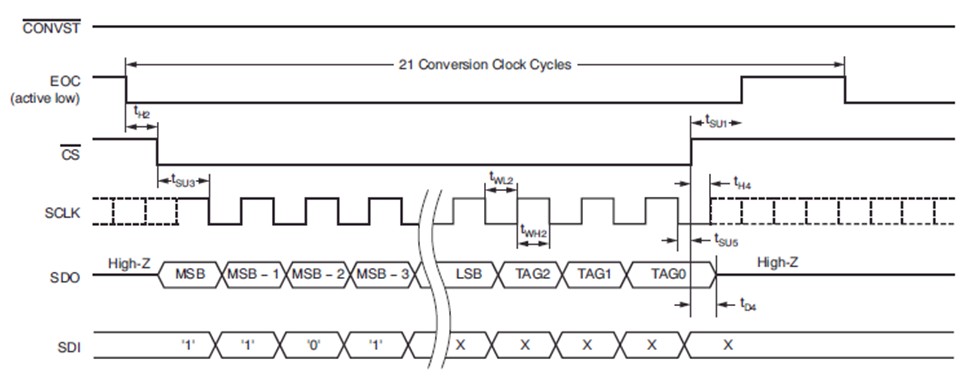
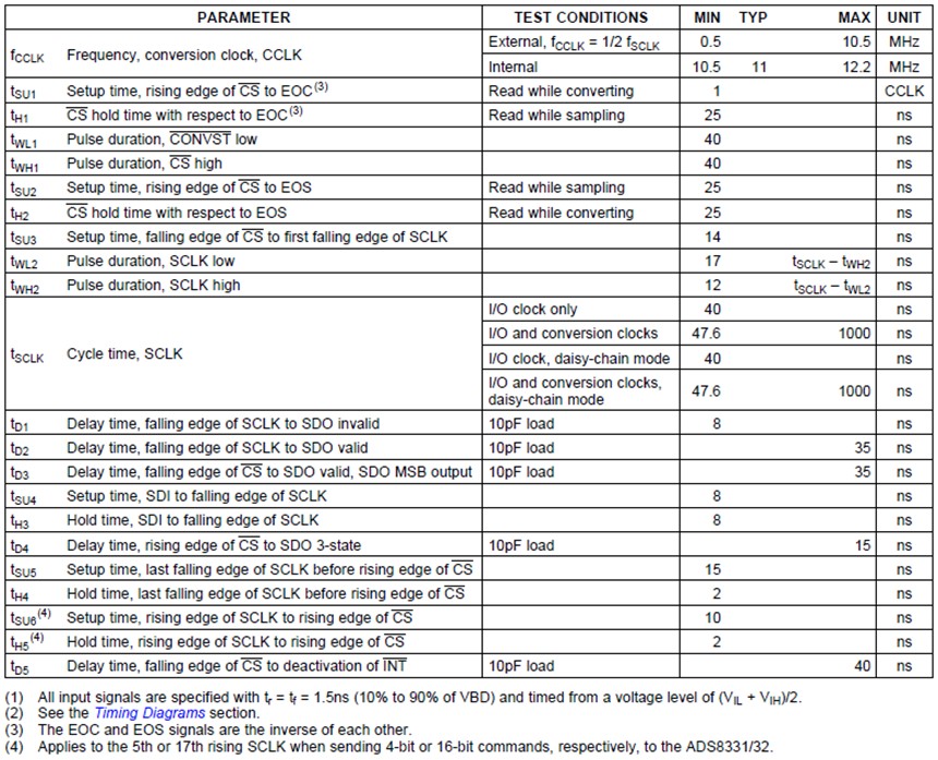
Figure 1 and Figure 2 are taken directly from the TI ADS833x datasheet for quick referencing. These function as the primary source of information for the Streaming Configuration property node timing parameters. Note that Figure 2 shows the timing table for a 2.7 V supply and 1.65 V digital reference. The datasheet also includes a table for a 5 V supply and 5 V digital reference. The TI ADS833x is using a 5 V supply, but because the digital reference from the NI USB-8452 is 3.3 V, you should not use the 5 V table. The lower digital reference voltage increases the setup/hold times (as seen in the 1.65 V table), which is why the table in Figure 2 is used.
Figure 1: Timing diagram for Auto-Trigger Mode from TI ADS833x datasheet (page 9)
Figure 2: Timing characteristics for TI ADS833x at 2.7V from datasheet (page 7)
SPI Stream Configuration Property Node
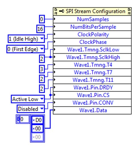
The SPI Stream Configuration property node sets all timing and line parameters for communication using the SPI Stream API. This node is also used to set the number of bits per transaction, the number of transactions, and the MOSI data for the SPI stream. You must configure all parameters the device requires to be interfaced with using this property node. Use the device’s datasheet to determine these requirements. The following sections explain how to use the TI ADS833x datasheet to identify and configure the property node parameters for the TI ADS833x EVM example. The resulting SPI Stream Configuration property node is shown Figure 3.
Figure 3: SPI Stream Configuration property node for TI ADS833x EVM example
Configuring CONV, DRDY, and CS
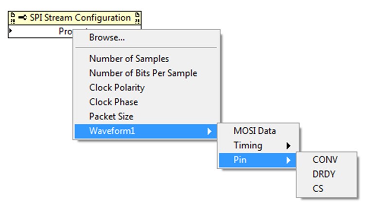
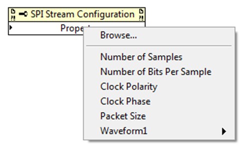
Not all devices use the CONV, DRDY, and CS lines. For our example, we will configure these lines for the mode established in the Introduction. Figure 4 shows the menu for selecting these lines in the property node.
Figure 4: Selecting CONV, DRDY, and CS in the SPI Stream Configuration property node
The CONV (convert) line is used to tell a slave device to start an operation. This line is also referred to as start or conversion start. You can configure the property node parameter to be active high/low, driven high/low, or disabled. Using the Start of a Conversion section (page 22) of the TI ADS833x datasheet, the CONV line (referred to as CONVST) is not required when the TI ADS833x is configured for Auto-Trigger mode. You also can see this in Figure 1 (note that CONVST never changes). CONV is therefore set to Disabled in the example.
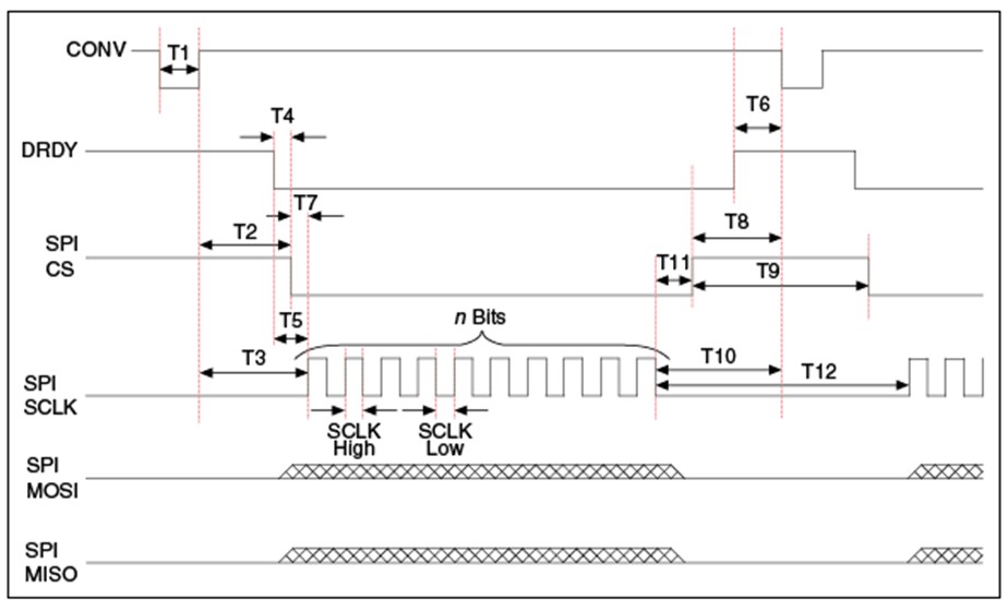
The slave uses the DRDY (data ready) line to inform the master that it has new data available for transfer. This line is also referred to as status or end-of-conversion. The slave drives it, and it is asynchronous to the master. You can configure the property node parameter to be active high/low or disabled. Using the Status Output Pin (EOC/INT) section (page 22) of the TI ADS833x datasheet, the DRDY line (referred to as EOC/end-of-conversion) is set to active low. You also can see the active low configuration in the diagram in Figure 1. DRDY is therefore set to Active Low in the example. Note that in Figure 9, it appears that DRDY timing parameters are edge sensitive (T6 for example). DRDY is actually level sensitive, meaning that when it is time to check whether DRDY is asserted/deasserted, an edge is not looked for; only the current voltage level is looked for. DRDY is checked only when the preceding timing parameters have been met. This means DRDY is not monitored when data is being transmitted or when the NI USB-8452 is toggling CS/CONV.
The master uses the CS (chip select) line to select which slave is active on the bus. This line is also referred to as slave select. You can configure the property node parameter to be active high/low, driven high/low, or disabled. Using the diagram in Figure 1, the CS line is configured as active low (note the bar over CS). CS is therefore set to Active Low in the example.
Determining Clock Phase and Polarity
The clock phase determines whether the data bits on the MOSI/MISO lines are centered on the first or second edge of the clock period. The clock polarity determines whether the clock line idles high or low. These parameters must be determined based on when the slave device is expecting data to be transmitted. The SPI clock is typically referred to as SCLK in datasheets. For our example, we will configure these lines for the mode established in the Introduction. Figure 5 shows the menu for selecting these lines in the property node.
Figure 5: Selecting Clock Phase and Polarity in the SPI Stream Configuration property node
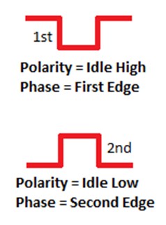
The Digital Interface section (page 27) of the TI ADS833x datasheet states that conversion data is valid and input data is read on the falling edge of SCLK. This means that the data must be centered on the falling edge of the clock. For this example, we have set the Clock Polarity to Idle High and Clock Phase to First Edge. Because the clock starts high, the first edge is the falling edge of the clock. An alternative implementation is to set the Clock Polarity to Idle Low and Clock Phase to Second Edge. In this implementation, the second edge is the falling edge because the clock starts low. Figure 6 shows these two implementations.
Figure 6: Two correct configurations of clock phase and polarity for TI ADS833x EVM example
Determining Necessary Timing Parameters
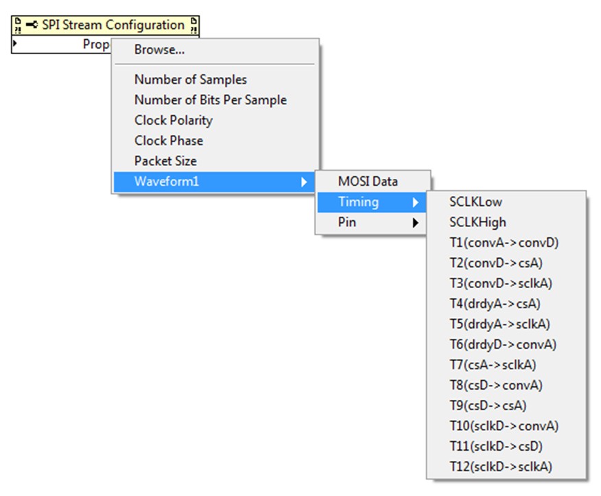
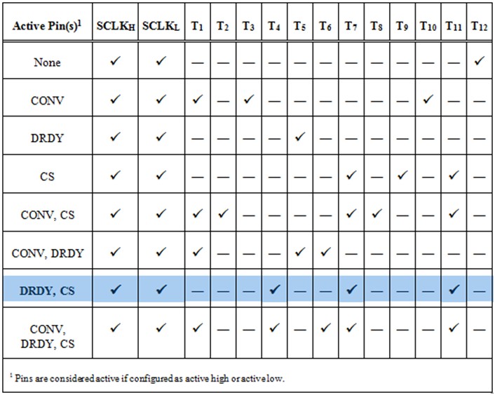
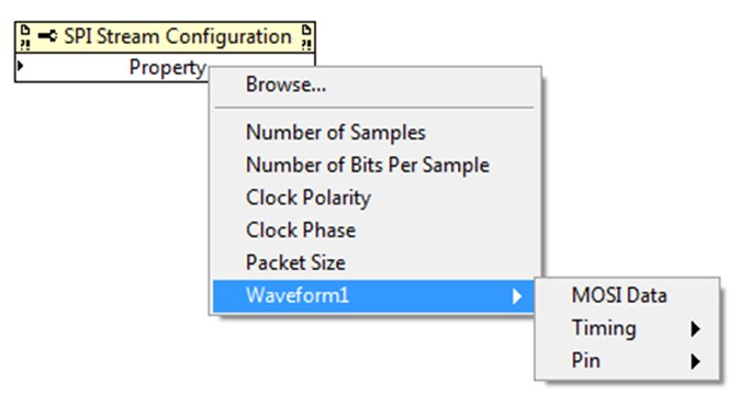
The timing parameters in the property node are set using multiples of the NI USB-8452 system clock. The Stream Mode section in the NI USB-845x Hardware Overview chapter of the NI-845x Hardware and Software Manual(3) states that the system clock for the NI USB-8452 is 10 ns. You can configure 14 possible timing parameters in the SPI Stream Configuration property node. Two of these are the high and low times for a single clock period (SCLKHigh and SCLKLow). SCLKHigh and SCLKLow always should be configured. The other 12 parameters (T1-T12) represent various hold and setup times for each line. You need to determine the values for these parameters using the datasheet. To determine which parameters you need to configure, use the Timing Parameters table in the Using the NI-845x SPI Stream API chapter of the NI-845x Hardware and Software Manual (shown in Figure 8). Note that the required timing parameters are determined by which of the CONV, DRDY, and CS lines are active. The Waveform 1 diagram (shown in Figure 9) from the same chapter shows which line timing the different parameters correspond to. Figure 7 shows the menu for selecting timing parameters in the property node.
Figure 7: Selecting timing parameters in the SPI Stream Configuration property node
Using the operating voltage and operation mode established in the Introduction, we can determine the timing parameters from the diagram shown in Figure 1 and the timing table in Figure 2. Because we have established that the TI ADS833x only uses the DRDY and CS lines (Configuring CONV, DRDY, and CS), the table (Figure 8) shows that we need to determine SCLKHigh, SCLKLow, T4, T7, and T11.
Figure 8: Timing Parameters table used to determine necessary parameters
Figure 9: Waveform 1 diagram showing which parameters correspond to which line timings
Using Figure 1, SCLKHigh corresponds to tWH2 and SCLKLow corresponds to tWL2. Figure 2 states that tWH2 requires a minimum of 12 ns and a maximum of tSCLK – tWL2 (tSCLK is the total clock period). The table also states that tWL2 requires a minimum of 17 ns and a maximum of tSCLK – tWH2. This means that the minimum SCLKHigh and SCLKLow parameter in multiples of the NI USB-8452 system clock is 2 (20 ns). To achieve maximum performance, SCLKHigh and SCLKLow are both set to 2.
T4 is the time from DRDY assert to CS assert. Using Figure 1, this time is labeled tH2. Figure 2 states that tH2 requires a minimum of 25 ns. This means T4 requires a minimum of 3 NI USB-8452 systems clocks, so T4 is set to 3 (30 ns) for maximum performance.
T7 is the time from CS assert to SCLK assert. SCLK assert is the clock edge corresponding to the first bit of data (this was determined in Determining Clock Phase and Polarity). Using Figure 1, this time is labeled tSU3. Figure 2 states that tSU3 requires a minimum of 14 ns. This means T7 requires a minimum of 2 NI USB-8452 systems clocks, so T7 is set to 2 (20 ns) for maximum performance.
T11 is the time from SCLK deassert to CS deassert. SCLK deassert is the clock edge corresponding to the last bit of data. Using Figure 1, this time is labeled tSU5. Figure 2 states that tSU5 requires a minimum of 15 ns. This means T11 requires a minimum of 2 NI USB-8452 systems clocks, so T11 is set to 2 (20 ns) for maximum performance.
Determining Number of Samples, Number of Bits Per Sample, and MOSI Data
Use the Number of Samples, Number of Bits Per Sample, and MOSI (master output slave input) Data parameters to set up SPI transaction data. Figure 10 shows the menu for selecting these parameters in the property node.
Figure 10: Selecting SPI transaction parameters in the SPI Stream Configuration property node
The Number of Samples parameter determines how many transactions occur after the stream is started. You can set this parameter to 0 to allow continuous streaming. Because we have chosen to sample a single channel continuously, we set Number of Samples to 0.
The Number of Bits Per Sample parameter determines how many bits are exchanged during each transaction. For our example, this is the number of bits exchanged for each conversion result. The Reading the Conversion Result section (page 29) of the TI ADS833x datasheet states that each conversion generates 16 bits of data. If TAG mode is enabled, the result will have 3 bits attached to the end of the conversion result that represent the channel the data is from. Because our example uses only a single channel, TAG mode is disabled. This means that 16 bits are exchanged per transaction, so NumBitsPerSample is set to 16.
The MOSI Data parameter determines the value of the bits sent from the master to the slave during a transaction. This parameter is an array of unsigned 8 bit integers. The master transfers the number of bits specified in Number of Bits Per Sample. If the array contains fewer bits than Number of Bits Per Sample, zeros are padded to the end. If the array contains more bits than Number of Bits Per Sample, the extra bits are not sent. Table 4 in the Digital Interface section (page 27) of the TI ADS833x datasheet shows that the first nibble (4 bits) transferred for a read should be 0xD (1101b). The remaining 12 bits are don’t cares. This means that MOSI Data could be an array containing only 1 element, 0xDX (1101XXXXb), and the second byte would be added automatically as 0x00. As a good programming practice, our example sets all 16 bits explicitly with the don’t cares being 0. MOSI Data is set to {0xD0, 0x00}. Note that the data is sent most significant byte (MSB) and most significant bit (MSb) first, which is why the data is contained in the upper nibble of the first byte of the array.
Resulting Waveform
You can view the resulting waveform for SPI transactions using a logic analyzer. Figure 11 shows the actual waveform produced by a single transaction from the TI ADS833x EVM example. Comparing this waveform against the timing diagram in Figure 1 shows that the SPI Stream Configuration has been set properly. Note that T4 is longer than the set 30ns because DRDY is an asynchronous signal and may require several NI USB-8452 cycles to be processed. You should not rely on this processing time for the minimum T4 timing.
Figure 11: Actual waveform produced from a single SPI Stream transaction
