LabVIEW Communications LTE Application Framework 2.0 and 2.0.1
Overview
Contents
Intro
The LTE Application Framework provides a ready-to-run, easily modifiable real-time physical layer (PHY) and lower medium access control (MAC)-layer reference design based on the LTE wireless standard. The LTE Application Framework is available with the LabVIEW Communications System Design Suite, also referred to as LabVIEW Communications.
This application framework provides a substantial starting point for researchers looking for ways to improve the LTE standard by exploring brand-new algorithms and architectures that can support the tremendous increase of the number of terminals, inventing new waveforms by which to modulate and demodulate the signals, or finding new multi-antenna architectures that fully exploit the degrees of freedom in the wireless medium.
The LTE application framework is comprised of modular PHY and MAC blocks implemented using LabVIEW Communications. It is designed to run on the powerful Xilinx Kintex-7 FPGA and an Intel x64 general purpose processor, which are tightly integrated with the RF and analog front ends of the NI software defined radio (SDR) hardware.
The framework is designed from the ground up for easy modifiability, while adhering to the main specifications of the LTE standard. This design allows wireless researchers to quickly get their real-time prototyping laboratory set up and running based on the LTE standard. They can then primarily focus on selected aspects of the protocol that they wish to improve, and easily modify the design and compare their innovations with the existing standards.
Scope
The LTE Application Framework provides the functional elements of the physical (PHY) layer as well as medium access control (MAC) layer of both base station (eNodeB) and user equipment (UE). This code includes the following elements:
- Downlink transmission (DL TX) and reception (DL RX)
- Uplink transmission (UL TX) and reception (UL RX)
Additionally, basic MAC functionalities are provided which allow for the following features:
- Packet-based user data transmission in downlink, enabling user data streaming applications
- Feedback of DL channel state information and DL (HARQ) ACK/NACK through the uplink
- Basic adaptive modulation and coding (AMC), which includes link adaptation in downlink, enabling DL closed loop operations
The following subsections describe in more detail which principal operation modes are provided by the LTE Application Framework and which specific subset of PHY and MAC functionalities of a 3GPP LTE release 10 compliant system is implemented.
Deviations and simplifications with respect to the 3GPP LTE release 10 standard are also described here. They have been applied to keep the complexity of the Application Framework at a reasonable level.
2.1 Operation modes
The LTE Application Framework offers three operation modes, as depicted in Figure 1. These three operation modes are provided by the following pairs of top-level host and top-level FPGA implementations:
Downlink (DL):
- Can be used to establish a downlink link in either a single-device setup or a double-device setup.
- Implements the downlink transmitter (DL TX) of a base station (eNodeB) and the downlink receiver (DL RX) of a user equipment (UE) including the basic DL TX and DL RX MAC functionalities
- In a single-device setup, a special MAC shortcut (see Figure 12 in section 3.1) allows for downlink AMC (rate adaptation) even without a real uplink feedback channel
- Top-level host VI: LTE Host DL.gvi
- Top-level FPGA VI is one of the following VIs:
- Version 2.0
- LTE FPGA FlexRIO DL.gvi
- LTE FPGA USRP RIO 40 MHz BW DL.gvi
- LTE FPGA USRP RIO 120 MHz BW DL.gvi
- Version 2.0.1
- LTE FPGA FlexRIO DL.gvi
- LTE FPGA USRP RIO DL.gvi
eNodeB:
- Provides the base station (eNodeB) side in a double-device setup.
- Implements the downlink transmitter (DL TX) and the uplink receiver (UL RX) of an eNodeB including the basic eNB MAC functionalities (see upper part of Figure 13)
- Top-level host VI: LTE Host eNodeB.gvi
- Top-level FPGA VI is one of the following VIs:
- Version 2.0
- LTE FPGA FlexRIO eNodeB.gvi
- LTE FPGA USRP RIO 40 MHz BW eNodeB.gvi
- LTE FPGA USRP RIO 120 MHz BW eNodeB.gvi
- Version 2.0.1
- LTE FPGA FlexRIO eNodeB.gvi
- LTE FPGA USRP RIO eNodeB.gvi
UE:
- Provides the user equipment (UE) side in a double-device setup
- Implements the downlink receiver (DL RX) and the uplink transmitter (UL TX) of a UE including the basic UE MAC functionalities (see lower part of Figure 13)
- Top-level host VI: LTE Host UE.gvi
- Version 2.0
- Version 2.0
Top-level FPGA VI is one of the following VIs:
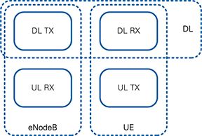
Figure 1: System configurations (host and associated FPGA code)
The downlink (DL) operation mode can be used either in a single-device setup or in a double-device setup. The eNodeB/UE operation modes require a double-device setup.
2.2 Physical Layer (PHY)
The LTE application framework implements parts of a 3GPP-LTE release 10 compliant downlink and uplink physical layer transmitter and receiver. To keep the complexity of this application framework at a reasonably low level, only a subset of the physical layer features defined for 3GPP-LTE release 10 compliant devices is implemented. This subset also includes feature simplifications and limitations of the configurability of the implemented PHY features, for example, specific configuration parameters are fixed to single values, and others are only quasi-statically configurable. Notice that fixed parameter settings can only be changed by modifying the design.
The following subsections give a detailed overview over the implemented PHY features, used simplifications, and (potentially restricted) PHY configuration capabilities with respect to the 3GPP LTE release 10 specifications.
2.2.1 Frame Structure , Bandwidth Mode, CP Mode and Physical Resource Grid
The LTE Application framework supports the following (partially fixed) configurations:
The detailed radio frame structure for both frame structure types is shown in Figure 2. Each radio frame is 10 ms long and consists of 10 subframes. Each subframe has a length of 1 ms, which comprises 30,720 complex time-domain baseband samples sampled at a rate of 30.72 MS/s, which is valid for the 20 MHz LTE bandwidth mode. The related sample period Ts is (1/30.72e6) s. The types of subframes vary with the subframe index in dependence on the selected radio frame type. Downlink subframes (D) are reserved for downlink transmissions; uplink subframes (U) are reserved for uplink transmissions. Special subframes (S) are used with frame structure type 2 (TDD) only. For TDD uplink-downlink configuration 5, which is supported by the LTE application framework, there is only one special subframe per radio frame. Special subframes consists of the following fields:
According to [1], the length of the special subframe fields varies with the special subframe configuration and the selected cyclic prefix configuration. In the current LTE Application Framework, implementation of both parameters are fixed to specific settings, so the special subframe fields have a fixed length.
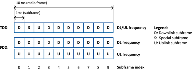
Figure 2: Subframe types for TDD and FDD Frame Structure
For normal cyclic prefix configuration, each subframe is divided into 14 OFDM symbols. The OFDM symbol duration is 2,048 * Ts extended by a cyclic prefix of 160 * Ts for OFDM symbols 0 and 7 and a cyclic prefix of 144 * Ts for all other OFDM symbols in a subframe.
For the 20 MHz LTE bandwidth mode, a 2,048-point IFFT is specified to be used in the OFDM modulator, in other words, 2,048 frequency-domain subcarriers per OFDM symbol are available. According to [1], only the inner 1,200 subcarriers, excluding the DC carrier, are allowed to be used for actual signal transmissions. The remaining unused subcarriers act as guard band to neighboring channels. The set of 1,200 usable subcarriers, also called resource elements, are organized in sets of 12 contiguous subcarriers corresponding to the physical resource blocks (PRBs). Notice that one PRB comprises the same set of 12 contiguous subcarriers, or resource elements, of multiple consecutive OFDM symbols, such as all OFDM symbols of a slot or subframe. For further details see [1].
2.2.2 Physical Downlink Channels and Signals
2.2.2.1 Overview
The downlink transmitter and receiver each include FPGA implementations of the following channels:
The following downlink channels and signals are not implemented:
The supported physical channels and signals are in general implemented in compliance with 3GPP LTE release 10 specifications [1], [2], [3]. Any specific deviations, extensions, simplifications, or configuration restrictions are explained in the corresponding sub-sections below.
2.2.2.2 Primary Synchronization Signal (PSS)
The PSS is transmitted only once per radio frame, with a periodicity of 10 ms instead of a periodicity of 5 ms. This adaption to the LTE specification is necessary to realize a unique detection of the radio frame start without SSS support. Depending on the selected frame structure type the PSS is transmitted in one of the following ways:
2.2.2.3 Cell-Specific Reference Signals (CRS)
CRS resource elements are always reserved (allocated) for two antenna ports. Active CRS transmissions are done on the first antenna port only.
2.2.2.4 UE-Specific Reference Signals (UERS)
UE-specific reference signals (UERS) can be optionally enabled in addition to CRS. The following features and configurations are supported:
If UERS are enabled, UERS-based channel estimates, instead of CRS-based channel estimates, are used by the downlink receiver to equalize the PDSCH.
Note: The UERS based channel estimation in the downlink receiver applies a simple interference cancellation scheme to reduce interference potentially caused by simultaneous code-orthogonal UERS transmissions on the same UERS resource elements. The underlying cancellation algorithm, which cannot be disabled in the current implementation, is designed for slowly time-varying radio channels only, which assumes the radio channel to be sufficiently time-invariant over a time period of one subframe (1 ms).
2.2.2.5 Physical Downlink Control Channel (PDCCH)
The PDCCH implemented in the LTE application framework mainly follows the specifications in [1], [2], [3], but is partially simplified and therefore is partially proprietary.
2.2.2.5.1 PDCCH Resource Grid
The LTE application framework allows the PDCCH to be transmitted only in the first OFDM symbol of each downlink or special subframe. This corresponds to a fixed control format indicator (CFI) of 1. All available (non-CRS occupied or reserved) resources are used for PDCCH, as PCFICH and PHICH are not part of the implementation.
2.2.2.5.2 PDCCH Format
The LTE standard allows for several different PDCCH formats (refer to [1] section 6.8.1), which differ in the so-called aggregation level, such as the number of consecutive control channel elements (CCEs) used for transmitting one downlink control information (DCI) message on the PDCCH. One CCE comprises nine resource element groups (REGs) with four resource elements (RE) per REG. Since the PDCCH is specified to use QPSK modulation, 2 bits per RE can be transmitted which finally comes to 72 bit per CCE.
The PDCCH format implemented in the LTE application framework is fixed to format 1, which corresponds to a fixed aggregation level of 2. Thus, 2 consecutive CCEs are always used to transmit one DCI message. This format corresponds to the allocation of 18 REGs (72 REs), which allows for the transmission of 144 encoded bits per DCI message.
2.2.2.5.3 DCI Format
The implemented downlink control information (DCI) format is partially proprietary. It corresponds to a subset of the LTE DCI Format 1. As illustrated in Figure 3, it consists of the following three fields:
Each bit of the PRB Allocation field represents 4 PRBs (according to DL resource allocation type 0, see [3] section 7.1.6.1). The leftmost bit represents the lowest resource block (group) index. The MCS signaling is compliant with the LTE standard, see [3] section 7.1.7. The supported MCS value range is restricted to 0...28. MCS 29, 30 and 31 are not supported as there is no HARQ processing included.

Figure 3: PDCCH DCI Format
Note: With the described DCI format only DL scheduling grants can be signalized using the PDCCH while uplink scheduling information are not supported to be sent with PDCCH. Thus, the uplink transmitter at the UE, as well as the uplink receiver at the eNB, must be configured manually using the respective host application.
The overall number of bits used for the supported DCI format is 32.
2.2.2.5.4 DCI Encoding
The DCI encoding mainly follows the 3GPP LTE release 10 specification. CRC attachment and channel coding are fully compliant with [2], but the rate matching is substituted by a simple parallel-to-serial conversion as is shown in Figure 4. According to [2], the LTE rate-matching block requires a subblock interleaver per parity bit output stream of the convolutional channel encoder, followed by a bit collection stage and a circular buffer, which is used for the actual rate adaptation (i.e. for bit puncturing (pruning) or repetition).
For the combination of the fixed PDCCH format (refer to section 2.2.2.5.2) and the fixed modified DCI format (see section 2.2.2.5.3) implemented by the LTE application framework, there is no need for any rate adaptation. The number of output bits delivered by the 1/3-rate convolutional channel encoder exactly matches with the number of bits that can be transmitted by the supported PDCCH format 1 (2 CCEs → 144bits). Thus, in this case the rate matching can be skipped.
Note: For reasons of simplicity the parallel-to-serial conversion implemented in the LTE Application Framework instead of the rate matching collects the parity output bits of the convolutional encoder as follows:

This equation is different than the way the bit collection stage is defined for the LTE-compliant rate matching. This stage collects the bits as follows:
where v i stands for the interleaved version of ith parity bit output stream dt of the channel encoder.
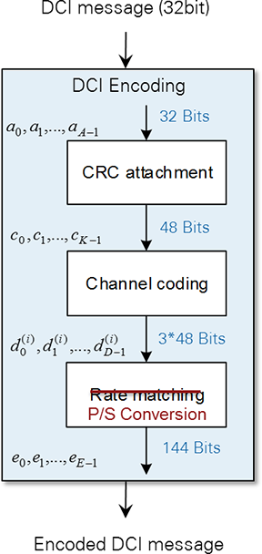
Figure 4: Modified DCI encoding scheme
2.2.2.5.5 PDCCH Multiplexing, Scrambling, Modulation, and Resource Mapping
Figure 5 shows the further PDCCH processing with the following functionalities:
It is implemented in compliance with the specifications in [1] with the following simplifications:

Figure 5: PDCCH processing
2.2.2.6 Physical Downlink Shared Channel (PDSCH)
Channel coding, scrambling, and modulation of the PDSCH are implemented in the LTE application framework in compliance with [1], [2] with the following restriction:
Layer mapping and precoding are implemented for transmission on single antenna port (transmission mode 1) only.
The PDSCH resource mapping is compliant with [1] with the following exceptions:
The LTE application framework supports a quasi-static PDSCH resource allocation at the downlink transmitter using resource allocation type 0 according to [3]. Thus, for the supported 20 MHz bandwidth mode 25 resource block groups (RBGs) can be individually allocated. Each RBG addresses a set of 4 consecutive PRBs.
The PDSCH modulation order and transport block size determination follows the specifications in [3] tables 7.1.7.1-1 and 7.1.7.2.1-1. They can be controlled at the downlink transmitter by means of the modulation and coding scheme (MCS) parameter. The LTE application frameworks supports all MCS between 0 and 28. MCS 29..31, which are only applicable with full DL HARQ support, are not implemented. For activated UERS MCS 28 is not supported since the resulting code rate would exceed 1 due to the modified UERS mapping.
Note: The selected PDSCH resource allocation as well as the selected modulation and coding scheme (MCS) are signaled to the downlink receiver via the PDCCH. Thus, the PDSCH configuration is applied automatically in the receiver and has not to be set manually.
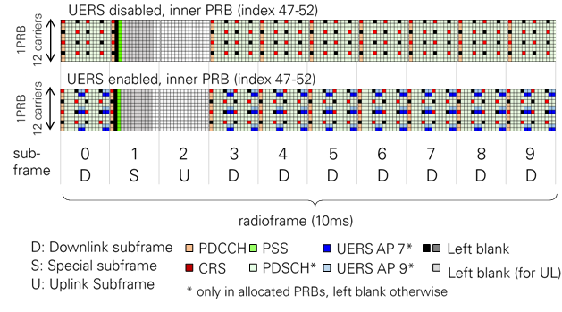
2.2.2.7 Supported DL resource grid
Figure 6 shows the resulting LTE downlink resource grid for frame structure type 2 (TDD) with all supported physical downlink channels and signals. It exemplarily shows the resource grid for the inner PRBs centered around DC which contain PSS. The resource mapping in the outer PRBs is in principle the same with the only difference that they do not contain PSS, instead the corresponding resource elements are left blank.
Figure 7 shows the resulting LTE downlink resource grid for frame structure type 1 (FDD) with all supported physical downlink channels and signals. The resource grid for both kind of PRBs, i.e. inner PRBs (containing PSS and PSS reserved REs) and outer PRBs (not containing PSS) are shown.
Figure 6: Supported LTE DL resource grid for frame structure type 2 (TDD)
Figure 7: Supported LTE DL resource grid for frame structure type 1 (FDD)
2.2.3 Physical Uplink Channels and Signals
2.2.3.1 Overview
The uplink implementation in the LTE application framework is using OFDMA instead of SC-FDMA. Neither the PUSCH DFT spreading nor the LTE uplink specific half subcarrier shift are applied. Simple OFDM modulation is used instead with a zero DC subcarrier inserted, similar to the LTE downlink specification.
The uplink transmitter and receiver implementations comprise the following physical channels and signals:
The following uplink channels and signals are not available:
2.2.3.2 Physical Uplink Shared Channel (PUSCH)
The PUSCH implemented in the LTE application framework applies a slightly simplified coding scheme in comparison to the specifications in [2]. The applied simplifications are illustrated in Figure 8. The resulting coding scheme is very similar to the coding scheme used for PDSCH. The specifics in comparison to full standard compliant PUSCH encoding are the following:
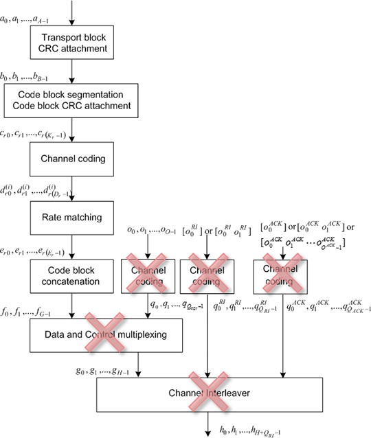
Figure 8: Simplified UL-SCH coding scheme
PUSCH scrambling, modulation, layer mapping, and pre-coding are implemented in compliance with [1] with the following restrictions:
The PUSCH transform precoding (DFT spreading) specified in [1] sec. 5.3.3 is not implemented since the LTE applications framework applies OFDM instead of SC-FDMA in the uplink.
The supported PUSCH resource mapping is compliant with the specifications in [1] with the following restrictions:
The LTE application framework supports a quasi-static PUSCH resource allocation at the uplink transmitter and uplink receiver using resource allocation type 0 according to [3]. Similar to the PDSCH allocation in the downlink 25 resource block groups (RBGs) can be individually allocated for PUSCH in uplink. Each RBG addresses a set of 4 consecutive PUSCH PRBs.
In the LTE application framework the PUSCH modulation order and transport block size determination uses the same MCS tables (see [3] Tables 7.1.7.1-1 and 7.1.7.2.1‑1) as applied for the PDSCH. This is a slight deviation from the LTE standard which originally defines a slightly different MCS scheme for the PUSCH. The MCS can be quasi-statically selected at the uplink transmitter and receiver in the range between 0 and 28.
Note: Since no uplink scheduling information is signaled from eNB to UE via the PDCCH, PUSCH resource allocation as well as PUSCH MCS have to be manually configured at both devices.
2.2.3.3 Demodulation Reference Signals (DMRS)
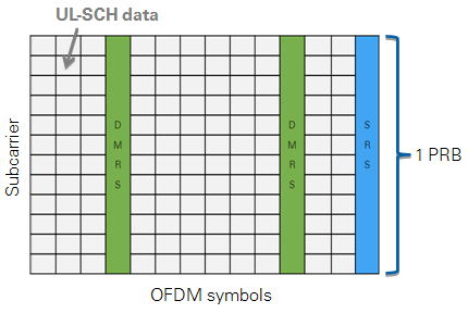
According to the LTE standard, DMRS are associated with the transmission of PUSCH or PUCCH. Since the LTE application framework does not provide a PUCCH implementation, only DMRS associated with PUSCH are supported. For the supported frame structure and the supported normal CP mode, DMRS are transmitted in the 4th and the 11th OFDM symbol of an uplink subframe, but only in those PRBs which carry PUSCH (see Figure 9).
The DMRS sequence generation implemented in the LTE application framework is slightly simplified in comparison to the specification in [1]. In deviation to the LTE standard DMRS sequences of different lengths (required for different numbers of allocated PUSCH PRBs) are all derived from one fixed base sequence defined for 100 PUSCH PRBs (i.e. for the maximum supported number of PUSCH PRBs). Shorter DMRS sequences are derived by taking the maximum length base sequence and cutting surplus symbols at the end. The base sequence generation itself is compliant with Sections 5.5.1 and 5.5.1.1 of [1]. The following fixed parameter set is applied for the base sequence generation.
Since the sequence-group number u and the base sequence number v are both fixed to 0, this implies that neither group hopping nor sequence hopping are supported.
2.2.3.4 Sounding Reference Signal (SRS)
In the LTE application framework uplink SRS support can be globally enabled or disabled. When SRS support is enabled, the last OFDM symbol in every UL subframe will be reserved for SRS transmissions, so it cannot be used for any other UL signal or channels anymore. This statement is true even if the uplink transmitter is not actively transmitting SRS in the corresponding uplink subframes. In TDD mode (frame structure type 2), the last 2 symbols of a special subframe can be used for SRS transmissions.
Active SRS transmissions can be individually scheduled for every UL subframe and every special subframe per radio frame. According to [1] section 5.5.3.3, this corresponds to
For this purpose a special parameter is provided at the control interfaces of the uplink transmitter and receiver. It is a bit vector with 10 elements, and each element addressing one specific subframe of a radio frame. In TDD mode, this bit vector will be masked with the supported pattern of special and uplink subframes to ensure that active SRS transmissions are only possible in these subframes. For individually addressing the 2 SRS symbols in the UpPTS field of a special subframe, the following rule is applied in TDD mode:
The used SRS bandwidth is always fixed to 96 PRBs, which corresponds to SRS bandwidth configuration C_SRS = 0 and SRS bandwidth B_SRS = 0.
The SRS transmission comb k_TC can be directly configured to be 0 or 1. SRS frequency hopping is not supported.
The SRS sequence generation is implemented in compliance with [1] section 5.5.3.1 and 5.5.1, but only the following fixed parameter set is supported.
As explained in section 2.2.3.3 for the DMRS, this implies that neither group hopping nor sequence hopping are supported.
The SRS transmitter is fully implemented. On the receiver side the SRS subcarrier data are extracted, but currently no further receiver operation is implemented.
2.2.3.5 Supported UL resource grid
Figure 9 shows the supported resource grid for an uplink subframe with active SRS.
Figure 9: Time-Frequency resource grid of an uplink subframe with enabled SRS support
2.2.3.6 Uplink transmit timing control
You can control the uplink transmit timing at the UE transmitter in a quasi-static manner using the uplink timing advance parameter. In the LTE application framework the uplink timing advance is set to zero per default. Zero means that the start of the transmitted uplink radio frame is fully aligned to the start of the received downlink radio frame at the UE antenna connectors. To cope with the propagation delay of real radio channels, the start of the uplink can be advanced by 0 up to 30,719 baseband samples (i.e. by 0...30,719xTs with Ts = 1/(30.72 MHz).
Note: [1] defines a fixed timing advance offset NTAoffset = 624xTs for frame structure type 2 (TDD). This offset is not automatically applied by the LTE application frame in TDD mode, but has to be set manually if needed.
In addition to the uplink timing advance mechanism, the LTE application framework autonomously corrects the UL transmit timing in relation to the downlink radio frame timing measured at the UE receiver. Thus, time tracking steps applied in the downlink receiver are also applied to the uplink transmitter. The time tracking is designed to cope with clock frequency differences between eNB and UE of up to ±5 ppm. Potential timing corrections are applied once per radio frame at the beginning of the radio frame.
They are realized by reducing or extending the cyclic prefix by an integer number of baseband samples. The current implementation allows for maximum correction steps of up to ±160 baseband samples (±160xTs). As long as the observed clock frequency difference is below the target maximum of ±5 ppm also the maximally applied timing correction step should be below ±2xTs, which is the upper limit defined by the LTE standard.
2.2.3.7 Uplink frequency offset correction
In addition to the autonomous UL transmit timing correction, the LTE application framework also applies an autonomous UL frequency offset correction. Carrier frequency offsets measured and corrected in the downlink receiver are also applied in the uplink transmitter with a carrier frequency depending scaling factor -1*fC,UL/fC,DL. Notice that frequency shifts in the uplink transmitter must be applied in the opposite direction as in the downlink receiver. For FDD, the ratio between uplink carrier frequency and downlink carrier frequency must be taken into account.
2.3 Medium Access Control Layer (MAC)
The LTE Application Framework implements the necessary functionality for establishing a link between the eNB (DL transmitter) and UE (DL receiver) and for enabling packet-based data transmission in the downlink. Furthermore it provides:
2.3.1 System Configuration
The system configuration is fixed to the following values at both the Downlink Transmitter (eNodeB) and Downlink Receiver (UE):
Because of the fixed configuration, System Information Block (SIB) transmission and reception is not needed and therefore not implemented.
2.3.2 Downlink Scheduling
The LTE application framework supports a quasi-static scheduling of the Physical Downlink Shared Channel (PDSCH) with respect to the resource block allocation. The PDSCH resource allocation can be controlled via a special control at the eNB (DL) transmitter. It will be valid as soon as and as long as the downlink transmitter is active. The PDSCH modulation and coding scheme (MCS) can be controlled by two alternative ways:
The Physical Downlink Control Channel (PDCCH) is used for signaling the PDSCH configuration (resource block allocation and MCS) from the eNB (DL) transmitter to the UE (DL) receiver. The signaling of the so called Downlink Control Information (DCI) is done for every downlink subframe and every special subframe. Since PDSCH transmissions in special subframes are currently not supported by the LTE application framework, no DCI message is transferred in those subframes.
Signaling the DCI via the PDCCH allows the UE (DL) receiver to be automatically configured to the PDSCH transmission parameters which might be dynamically selected by the eNB MAC. This is a pre-requisite for dynamic link adaptation (AMC) in the downlink.
In principle, LTE eNBs are designed to support multiple UEs. That’s why the cyclic redundancy check field (CRC) attached to the DCI messages during the encoding is mask with a UE specific radio network temporary identifier (RNTI). During the decoding of the PDCCH the UE receiver checks whether this CRC masks fits with the own RNTI or not. In case of any mismatch the DCI message will be discarded and the PDSCH data will not be decoded. This way the eNB can address a specific UE so that only this device decodes the PDSCH data. This also implies that for a successful downlink data transmission with the LTE application framework the RNTI selected at the eNB transmitter has to be identical to the RNTI set at the UE receiver.
2.3.3 Uplink Scheduling
Similar to the downlink, the uplink uses a quasi-static scheduling. For the physical uplink shared channel (PUSCH) both have to be configured manually, the resource block allocation as well as the MCS. Since the PDCCH does not support signaling of uplink scheduling information, both the eNB receiver as well as the UE transmitter have to be configured manually.
As described before the eNB downlink transmitter starts transmitting with (a quasi-statically selected configuration) as soon as it is switched on. Assumed the UE downlink receiver is configured accordingly (e.g. same carrier frequency, same frame structure, same reference symbol type etc.) it should be able to synchronize to the downlink transmitter and to receive and decode the downlink PHY channels. The same holds for the uplink. The UE transmits a quasi-statically configured uplink as soon as it switched on and the the eNB receiver should be able to receive and to decode the uplink transmission as long as it is configured correctly. All adjustable parameters like e.g. carrier frequency, frame structure, transmit power, and uplink timing advance have to be configured manually. Complex cell search or cell attachment procedures are not implemented.
2.3.4 Downlink MAC Packet for User-Defined Data
A simple MAC implementation (Mini MAC) is used to fill the transport blocks of the downlink shared channel with user-defined payload data. This way, the downlink can be used for packet-based data transmission.
The MAC packet format is proprietary and shown in Figure 10. The PDSCH transport block size is defined according to [3] tables 7.1.7.1-1 and 7.1.7.2.1-1. It depends on the used modulation and coding scheme (MCS) and the number of resource blocks allocated for the PDSCH.
For each subframe the simple MAC implementation checks the fill state of the payload data FIFO which is filled with user-defined data from the host. Depending on the buffer fill state and the number of PDSCH transport block bits usable in the current subframe, the MAC determines the number of payload bytes which can be effectively transmitted by the PDSCH transport block. Based on this the content of the actual PDSCH transport block is composed. It starts with a 4 byte long MAC header which contains the number of effectively transmitted payload bytes. The second part is the payload itself. If necessary zero padding bits are added to fill up the PDSCH transport block to the configured size.
Figure 10: MAC Packet Structure
2.3.5 Uplink MAC Packet for Feedback Information
The content of the uplink transport blocks is composed based on the same MAC packet format as it is described for the downlink (see Figure 10 above). The actual payload portion is filled with downlink feedback information. As shown in Figure 13, each payload portion of an uplink MAC packet comprises 6 words of 32 bits, i.e. 192 bits in total. Unused bits are set to zero.
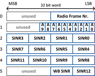
Figure 11: Feedback Information Packet Format
The feedback information is generated by the UE host implementation (UE feedback MAC) based on results provided by the UE downlink receiver. The following feedback information is provided:
2.3.5.1 SINR estimation algorithm
The SINR estimation algorithm is based on filtering the potentially noise channel estimates derived for the CRS subcarrier or the UERS subcarrier, respectively.
The noisy least squares (LS) channel estimates obtained for the reference symbol carriers are filtered by a de-noising low-pass filter to obtain LS channel estimates with reduced noise. The implemented prototype de-noising filter is a raised cosine filter with 9 taps and the following filter coefficients.
| Coefficient Index | Coefficient Value |
|---|---|
| 0 | 0 |
| 1 | -0,061235467 |
| 2 | 0 |
| 3 | 0,306177333 |
| 4 | 0,510116268 |
| 5 | 0,306177333 |
| 6 | 0 |
| 7 | -0,061235467 |
| 8 | 0 |
The averaged signal power of the difference between the noisy channel estimates and their low-pass filter complements can be taken as raw estimate for the noise variance, i.e. it can be considered as scaled version of the actual noise variance in the given frequency band or sub-band.
Averaging the squared magnitudes of the low-pass filtered channel estimates delivers a raw estimate of the mean channel power gain.
Based on the known reference signal transmit power, the raw estimate of the mean channel power gain, and the raw estimate of the noise variance a raw CINR estimate can be derived.
Because both the raw mean channel power gain estimates and the raw noise variance estimates are biased, the raw SINR estimates are biased. Notice that especially the bias of the noise variance estimates bias strongly depends on the actual noise variance. That's why a mapping function has to be applied to map the biased raw SINR estimates to the final unbiased SINR estimates.
This mapping function has been derived by means of calibration simulations and measurements. It has been approximated by the set of the following 2 linear functions (valid for a target SINR range between -6...30dB):
- Version 2.0
- LTE FPGA FlexRIO UE.gvi
- LTE FPGA USRP RIO 40 MHz BW UE.gvi
- LTE FPGA USRP RIO 120 MHz BW UE.gvi
- Version 2.0.1
- LTE FPGA FlexRIO UE.gvi
- LTE FPGA USRP RIO UE.gvi
- Bandwidth mode: 20 MHz (100 PRBs)
- Cyclic prefix configuration: Normal cyclic prefix
- Frame Structure:
- Type 1 – FDD
- Type 2 – TDD
- TDD uplink-downlink configuration: 5
- Special subframe configuration: 5
- DwPTS – Downlink pilot time slot
- Reserved for downlink transmission
- In the LTE Application Framework, it is restricted to transmission of Physical downlink control channel (PDCCH) and cell-specific reference signals (CRS)
- Length: fixed to 3 OFDM symbols (6,592 * Ts)
- GP – Guard Period
- Time-domain guard period for switching between active downlink transmission/reception and active uplink reception/transmission
- Length: fixed to 9 OFDM symbols (19,744 * Ts)
- UpPTS – Uplink pilot time slot
- Reserved for transmission of uplink sounding reference symbols (SRS)
- Length: fixed to 2 OFDM symbols (4,384 * Ts)
- Primary Synchronization Signal (PSS)
- Cell-Specific Reference Signals (CRS)
- UE-Specific Reference Signals (UERS)
- Physical Downlink Control Channel (PDCCH)
- Physical Downlink Shared Channel (PDSCH)
- Secondary Synchronization Signal (SSS)
- MBSFN reference signals
- Positioning reference signals
- CSI reference signals
- Physical Control Format Indicator Channel (PHICH)
- Physical Hybrid-ARQ Indicator Channel (PCFICH)
- Physical Broadcast Channel (PBCH)
- Physical Multicast Channel (PMCH)
- The third OFDM symbol of subframe 1 for TDD
- The seventh OFDM symbol of subframe 0 for FDD
- Supported on antenna ports 7 to 14; not supported on antenna port 5
- Supported in downlink subframes only; not supported in special subframes
- Sequence generation as specified in [1] for antenna ports 7 to 14
- Implemented for the nSCID parameter fixed to 0 (can be changed in sequence generation module)
- With UERS support enabled the resource elements for both UERS antenna port sets {AP 7, 8, 11, 12} and {AP 9, 10, 13, 14} are reserved in each slot of a downlink subframe while active UERS transmission and reception is only performed for the selected antenna port.
Notice that this is a deviation from (an extension to) the 3GPP LTE specification [1] and would be a prerequisite for TM9, like multiuser MIMO for up to 8 UEs.
- PRB—allocation for signaling the PRB allocation for the PDSCH
- MCS—for signaling the PDSCH modulation and coding scheme
- TPC—reserved for e.g. uplink transmit power control commands, currently not used
- PDCCH multiplexing
- Scrambling
- Modulation
- Layer mapping and precoding
- Mapping to resource elements
- PDCCH multiplexing currently supports only 1 control channel (DCI message) to be transmitted per subframe
- There are eight possible CCE positions, which are pairs of consecutive CCEs, that can be manually selected via the CCE offset parameter prerequisite for multi-user support for up to 8 UEs
- No support of automatic CCE selection (PDCCH assignment) in dependence on RNTI and search space (as defined in [3] section 9.1.1). No need of blind PDCCH decoding procedures in the DL receiver
- QPSK modulation as specified in [1], but for reasons of implementation efficiency modulation is performed after the REG interleaving
- Note: This specific implementation does not influence the final output of the overall PDCCH processing.
- Layer Mapping and precoding are supported for transmission on a single antenna port (transmission mode 1) only
- Since this is a one-to-one mapping, the block has not to be implemented at all.
- REG interleaving supported for fixed Cell-ID value 0 only
- For this Cell-ID value the cell-specific cyclic shift, which is specified in [1] in addition to the actual interleaver functionality, becomes transparent and therefore is not implemented.
- HARQ support is not implemented
- PDSCH transmission is supported in downlink subframes only; not supported in special subframes.
- The PDSCH resource mapping is adapted to the modified or restricted resource mapping of PSS, CRS, and UERS.
- Resource elements outside the PDCCH region available from channels and signals which are not implemented (e.g. SSS, PBCH) are used for PDSCH.
- For activated UERS PDSCH is not transmitted in resource blocks in which parts of the UERS (due to potential overlap with other PHY channels or signals) are not transmitted.
- This restriction currently applies for frame structure type 1 (FDD) where the PRBs centered around DC in subframe 0 are not used for PDSCH transmissions due to the potential overlap with the PSS.
- To ease the handling for the user the related conditions will be automatically checked by the FPGA implementation of the downlink transmitter and the PDSCH resource allocation will be automatically modified for the affected subframes. The modified PDSCH resource allocation will be applied for the whole PDSCH processing (including the transport block size determination) as well as for the related DCI content signaled on the PDCCH. As the currently implemented DCI format only allows for signaling the allocation of 4 consecutive PRBs, not only the 6 PRBs colliding with PSS but in total the 12 innermost PRBs will not be used for PDSCH transmission in this special case.
- Physical Uplink Shared Channel (PUSCH)
- Demodulation Reference Signals (DMRS)
- Sounding Reference Signal (SRS)
- Physical Random Access Channel (PRACH)
- Physical Uplink Control Channel (PUCCH)
- Only the coding for the Uplink Shared Channel (UL-SCH) data is supported
- Coding and multiplexing of Uplink Control Information (UCI) on PUSCH is not supported
- Layer mapping and precoding are implemented for transmission on single antenna port only.
- For activated SRS support the last OFDM symbol cannot be used for PUSCH at all, even if the UE is not actively transmitting SRS.
- PUSCH transmission are only allowed on contiguous resource block sets.
- Uplink frequency hopping (PUSCH hopping) is not implemented.
- srs-SubframeConfig = 0 for FDD
- srs-SubframeConfig = 7 for TDD in general, (which is also equivalent to srs-SubframeConfig = 1 for TDD5/5)
- The bit related to a special subframe controls SRS transmissions in the last OFDM symbol of the special subframe.
- The bit related to the DL subframe preceding a special subframe controls SRS transmission in the previous last OFDM symbol of that special subframe
- Feedback of DL channel state information and DL (HARQ) ACK/NACK via the uplink
- Basic adaptive modulation and coding (AMC), known as link adaptation in downlink, enabling DL closed loop operations
- Bandwidth: 20 MHZ (100 PRBs)
- Control Format = 1 (PDCCH spans over one OFDM symbol per subframe)
- Antenna configuration: single antenna (SISO)
- Quasi-statically by means of a special control at the downlink transmitter (eNB)
- Automatically by means of the rate adaptation functionality of the DL MAC
- Based on the DL channel state feedback information (wideband SINR) received via the uplink the DL MCS will be adapted to obtain a default target BLER at the downlink receiver of about 5-10%.
- A special parameter SINR offset [dB] can be used to indirectly control the target downlink BLER by reducing the reported SINR by the given value before it is fed into the rate adaptation framework.
- Radio Frame Number: A counter value from 0 to 1023 which is increased for each radio frame. It corresponds to the system frame number (SFN) defined in the LTE standard with the difference, that the timing is generated on the UE side and not dictated from the eNodeB using system information
- A0 – A9: the DL ACK/NACK/DTX information for the latest 10 subframes providing information about the success of the PDSCH reception. The values are encoded as a 2 bit number:
- 0 = NACK (PDSCH was received with CRC error)
- 1 = ACK (PDSCH was received with CRC ok)
- 2 = DTX (no PDSCH was decoded because of missing or invalid DCI message)
- 3 = undefined
- Subband and wideband signal-to-interference noise ratio (SINR) in dB
- Subband size used for SINR calculation: 8 PRBs
- Subband numbering:
- SINR0 is the subband SINR for PRBs 0..7, SINR1 for PRBs 8..15, etc.
- SINR WB is the wide band SINR calculated over all subbands
- Fixed point format: 8 bits signed fixed-point number with 6 integer and 2 fractional bits (range -32.00 dB to +31.75 dB)
- SINR calculation is based on the CRS- or UERS-based channel estimates provided by the downlink receiver. Refer to section 2.3.5.1 for more details.
- When using UERS the resource block allocation is currently not taken into account for SINR calculation. As UERS are only transmitted on allocated PRBs, SINR calculation results on not or only partially allocated subbands are undefined (i.e. in most cases less than the actual channel quality). Wideband SINR value is also undefined if not all subbands are fully occupied.
- SINR/dB = 1.8*SINRraw/dB - 10.2 for -6 ≥ SINRraw/dB < 6
- SINR/dB = 1.1*SINRraw/dB - 6 for 6 ≤ SINRraw/dB ≤ 30
Note: To further improve the provided SINR estimates, an additional look-up table based fine-calibration stage is implemented in the LTE application framework. The underlying look-up table has been derived by fine-calibration measurements.
- SINR/dB = 1.1*SINRraw/dB - 6 for 6 ≤ SINRraw/dB ≤ 30
Implementation Details
3.1 Architectural Overview
Figure 12 and Figure 13 show the block diagram of the system in the DL, eNodeB, and UE operation modes. Data streams that require high data rates for data transfer between host and FPGA are implemented as DMA FIFOs. These streams include the payload and uplink data from host to FPGA and the received PDSCH/PUSCH transport blocks from FPGA to host. I/Q samples for constellation and spectrum display as well as the channel estimation values are also transferred from FPGA to host using DMA FIFOs. Further status information is transferred to the host by reading the indicator values.
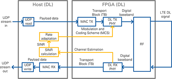
Figure 12: Block diagram of the system in DL operation mode (single-device setup)
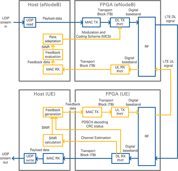
Figure 13: Block diagram of the system in eNodeB/UE operation mode (double-device setup)
The components shown in Figure 12 and Figure 13 perform the following tasks:
- UDP read: Reads data, provided by an external application, from a UDP socket. The data is used as payload data in the Transport Block (TB), which is then encoded and modulated as a LTE downlink (DL) signal by the downlink transmitter (DL TX PHY).
- UDP write: Writes the payload data, which was received and decoded from the LTE downlink (DL) signal by the downlink receiver (DL RX PHY), to an UDP socket. The data can then be read by an external application.
- MAC TX: A simple MAC implementation which adds a header to the Transport Block (TB) containing the number of payload bytes. The header is followed by the payload bytes and the remaining bits of the Transport Block are filled with padding bits.
- MAC RX: Disassembles the Transport Block (TB) and extracts the payload bytes.
- DL TX PHY: Physical layer (PHY) of the downlink (DL) transmitter (TX). Encodes the physical channels and creates the LTE downlink signal as digital baseband I/Q data. This includes: encoding of the control channel (PDCCH), encoding of the data channel (=shared channel, PDSCH), resource mapping, and OFDM modulation.
- DL RX PHY: Physical layer (PHY) of the downlink (DL) receiver (RX). Demodulates the LTE downlink signal and decodes the physical channels. This includes: primary synchronization sequence (PSS) based synchronization, OFDM demodulation, resource demapping, channel estimation & equalization, decoding of the control channel (PDCCH), and decoding of the data channel (=shared channel, PDSCH).
- UL TX PHY: Physical layer (PHY) of the uplink (UL) transmitter (TX). Encodes the physical channels and creates the LTE uplink signal as digital baseband I/Q data. This includes: encoding of the data channel (=shared channel, PUSCH), resource mapping, and OFDM modulation.
- UL RX PHY: Physical layer (PHY) of the uplink (UL) receiver (RX). Demodulates the LTE downlink signal and decodes the physical channels. This includes: OFDM demodulation, resource demapping, channel estimation & equalization, and decoding of the data channel (=shared channel, PUSCH).
- SINR calculation: Calculation of the Signal-to-Interference-Noise-Ratio (SINR) based on the channel estimation which was used for PDSCH decoding: channel estimation is either based on cell-specific reference signals (CRS) or on UE-specific reference signals (UERS)
- Rate adaptation: Sets the Modulation and Coding Scheme (MCS) depending on the measured/reported Signal-to-Interference-Noise-Ratio (SINR). The aim is to ensure to keep the block error rate (BLER) of the PDSCH decoding low.
- Feedback generation: Creates a feedback message with contains the measured subband and wideband SINR as well as the ACK/NACK information (=CRC result of the PDSCH decoding) of the previously received radio frame.
- Feedback evaluation: Extracts the subband and wideband SINR as well as the ACK/NACK information from the feedback message.
3.2 FPGA Implementation Overview
This LTE Application Framework is based on the target-specific sample streaming project:
- Version 2.0—PXIe USRP RIO 40 MHz BW Single-Device Streaming for USRP RIO 40 MHz BW or PXIe USRP RIO 120 MHz BW Single-Device Streaming for USRP RIO 120 MHz BW or PXIe NI-579xR Streaming for FlexRIO
- Version 2.0.1—PXIe USRP RIO 120 - 160 MHz BW Single-Device Streaming for USRP RIO or PXIe NI-579xR Streaming for FlexRIO
The sample streaming project contains the basic logic to interface with the analog-to-digital converter (ADC) and digital-to-analog converter (DAC) registers. It also performs digital up and down conversion, configuration for the front-ends, and RF impairment correction.
In the LTE Application Framework, the processing blocks for the downlink and uplink transmitter and receiver are implemented on the FPGA directly. They exchange the baseband data with the RF interface using target-scoped FIFOs. The processing on the FPGA has advantages as it provides lower latency and therefore enables real-time physical layer processing. This approach is different from the sample streaming project where the digital baseband data is sent to or received from the host which is then responsible for all channel encoding and decoding.
Figure 14 shows the structure of the FPGA implementation for the different operation modes. The outer boxes (highlighted in light gray) represent single-cycle timed loops which implement clock-driven logic. The inner boxes correspond to the high-level blocks described in the architectural overview. The transmitter loop receives payload data from the host via a DMA FIFO, performs channel encoding and generates the TX baseband signal which is passed to the RF loop for up conversion. The RF loop is inherited from the sample streaming project. It also performs down conversion of the RX baseband signal that is passed to the receiver loop for channel decoding. The decoded transport blocks are sent to the host using a DMA FIFO.
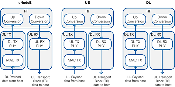
Figure 14: Implemented FPGA Loops for Different Operation Modes
3.2.1 RF Interface
3.2.1.1 Digital Upconversion and RF Impairment Correction
The transmit part of the RF loop is shown in Figure 15. The first block is the Fractional Interpolator which converts the standard LTE rate of 30.72 MS/s to the DAC sample rate (120 MHz for USRP RIO 40 MHz BW, 200 MHz for USRP RIO 120 MHz BW or 160 MHz BW, 130 MHz for FlexRIO). Next, the frequency shift module performs a fine frequency shift which is automatically configured by the RF driver. The I/Q imbalance correction uses coefficients determined during manufacturing and stored in the device EEPROM.

Figure 15: Digital Upconversion Block Diagram
3.2.1.2 Digital Downconversion and RF Impairment Correction
The receive part of the RF loop is shown in Figure 16. It corrects I/Q impairments in the baseband signal, performs fine-frequency adjustments, and performs sample rate conversion. I/Q imbalance correction uses coefficients determined during manufacturing and stored in the device EEPROM. A decimator converts the sample rate from the ADC sample rate (120 MHz for USRP RIO 40 MHz BW, 200 MHz for USRP RIO 120 MHz BW or 160 MHz BW, 130 MHz for FlexRIO) to the standard LTE rate of 30.72 MS/s. The LTE Application Framework also includes a DC suppression to compensate for the DC offset. This module averages over time to remove the DC portion of the signal.

Figure 16: Digital Downconversion Block Diagram
3.2.2 Downlink Transmitter
3.2.2.1 Overview
The Downlink Transmitter is implemented by the FPGA top-level variants eNodeB and Downlink only (DL). In the block diagrams of Figure 12 and Figure 13, it corresponds to the DL TX PHY block.
As shown in the simplified block diagram in Figure 17, it performs the following tasks:
- Physical Downlink Control Channel (PDCCH) encoding
- Physical Downlink Shared Channel (PDSCH) encoding
- Mapping to resource elements (EDSC architecture, see section 5.1.1)
- iFFT conversion + CP conversion (OFDM modulation)
The following reference signals and physical channels are mapped:
- Primary Synchronization Signal (PSS)
- Cell-Specific Reference Signal (CRS)
- UE-specific Reference Signal (UERS), if enabled
- Physical Downlink Control Channel (PDCCH)
- Physical Downlink Shared Channel (PDSCH)
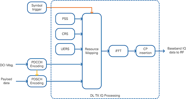
Figure 17: Simplified Block Diagram of Downlink Transmitter
Channel Encoding is performed for the PDCCH and PDSCH physical channels as shown in Figure 18. The encoding is performed for each downlink subframe by the FPGA implementation which allows real-time operation. The other signals are read out from look-up tables (LUTs).
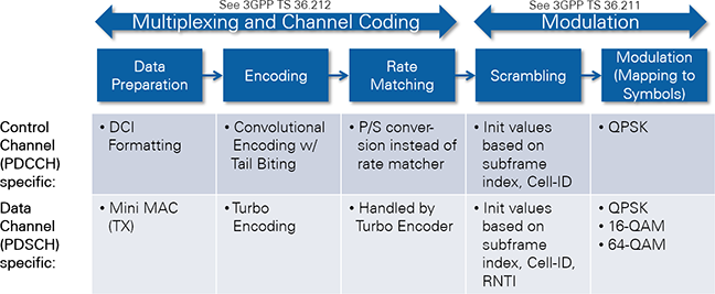
Figure 18: Channel Encoding performed in the Downlink Transmitter
3.2.2.2 FPGA Implementation Details
An extended block diagram which represents the actual implementation is shown in Figure 19. It shows the data path (blue), the configuration signals (yellow) and the triggering signals (orange).
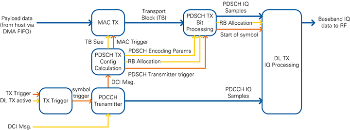
Figure 19: Block Diagram of Downlink Transmitter showing Data, Trigger and Control Paths
If the Downlink Transmitter is active and if it receives a TX trigger signal, it generates symbol triggers for one complete radio frame (10 subframes à 14 symbols = 140 symbols). The TX trigger signal is provided from a register which is written in the DAC/ADC loop. This ensures synchronization between both loops and compensates eventual clock drifts. The symbol trigger is passed through the rest of the chain and causes the modules to produce data: a subframe trigger is derived for the PDCCH and PDSCH Transmitters which produce enough data for one subframe. The DL TX I/Q uses the symbol trigger and generates time-domain I/Q samples for one OFDM symbol.
The PDCCH Transmitter performs channel encoding for the physical downlink control channel (PDCCH). The DCI message serves as input data. As shown in Figure 3 it contains the modulation and coding scheme (MCS) and the resource block allocation (RB Allocation). The resulting PDCCH I/Q samples are written to a FIFO inside the TX I/Q Processing module.
The DCI message is also input to the module which calculates the PDSCH transmitter configuration parameters (PDSCH TX Config Calculation). It performs two tasks: first, it calculates the transport block (TB) size and triggers the MAC TX. Second, it calculates the PDSCH Encoding parameters, extracts the resource block (RB) allocation and triggers the PDSCH TX Bit Processing module.
The MAC TX assembles the transport block in the format as shown in Figure 10. The payload data is read from the host via a host-to-target DMA FIFO.
The PDSCH TX Bit processing module includes the channel encoding, scrambling, and modulation of the physical downlink shared channel (PDSCH). It uses the modulation and coding scheme (MCS) which is defined inside the DCI message. The resulting PDSCH I/Q samples are written to a FIFO inside the TX I/Q Processing module.
The TX I/Q processing module is triggered after the PDCCH and PDSCH I/Q samples for the current subframe were generated. It includes the resource mapping that assembles all 1200 subcarriers of the current symbol. The index generator generates the timing information for each sample of the current OFDM symbol, such as subcarrier, resource block, OFDM symbol and subframe index. Depending on the current timing information, the index-to-channel mapping decides for each subcarrier, which reference signal or physical channel is mapped to it. The PSS sync sequence, the cell-specific reference symbols (CRS) and the UE-specific reference symbols (UERS) are precalculated and stored in a look-up table (LUT). The PDCCH and PDSCH I/Q samples are read from a FIFO which was filled with all I/Q samples for the current subframe before the TX I/Q processing module was triggered. After combining all channels, the DC gap is inserted and whitespace is added so that the resulting number of samples equals the FFT size of 2048. The inverse fast Fourier transformation (iFFT) converts the frequency domain data into the time domain. Finally, the cyclic prefix is attached to the output of the iFFT. The resulting time-domain signal is transferred to the RF loop using a FIFO.
3.2.2.2.1 PDCCH Transmitter
The PDCCH Transmitter creates all QAM symbols for the PDCCH channel. The contained blocks are illustrated in Figure 20.
Upon reception of the symbol trigger, the DCI message is generated based on the configuration from the host. The message is encoded and a CRC is attached. The DCI multiplexer module shifts the generated symbols to the correct position within the PDCCH channel. Afterwards the whole channel data is scrambled and interleaved. After applying the QPSK-Modulation to the symbols, the PDCCH I/Q-samples are fed into a FIFO that stores them until they are picked up by the resource grid generation.

Figure 20: PDCCH Transmitter Block Diagram
3.2.2.2.2 PDSCH Transmitter
The PDSCH transmitter converts the user data from the host to QAM symbols for the PDSCH channel. The blocks of this processing chain are shown in Figure 21.
A basic MAC implementation adds a proprietary MAC header to the beginning of each PDSCH transport block. The remaining transport block is filled with as much user data as available from the host FIFO. If necessary, zero padding bits are added to fill the remaining portion of the transport block. The PDSCH Encoder uses the LTE PxSCH Channel Encoder described in section 5.2. The output of the core is scrambled according to the LTE specification. Afterwards the QAM modulation is applied. The MCS value on the host sets the modulation scheme. After the modulation, the PDSCH QAM symbols are fed into a FIFO that holds these values until they are pulled into the resource grid.

Figure 21: PDSCH Transmitter Block Diagram
3.2.3 Downlink Receiver
3.2.3.1 Overview
The Downlink Receiver is implemented by the FPGA top-level variants UE and Downlink only (DL). As shown in the simplified block diagram in Figure 22, it performs the following tasks:
- Synchronization and carrier frequency-offset (CFO) compensation
- CP removal + FFT conversion (OFDM demodulation)
- Demapping of the resource elements to the different physical channels
- CRS-based channel estimation and equalization
- UERS-based channel estimation and equalization
- Physical Downlink Control Channel (PDCCH) decoding
- Physical Downlink Shared Channel (PDSCH) decoding
The following reference signals and physical channels are demapped:
- Primary Synchronization Signal (PSS)
- Cell-Specific Reference Signal (CRS)
- UE-specific Reference Signal (UERS)
- Physical Downlink Control Channel (PDCCH)
- Physical Downlink Shared Channel (PDSCH)

Figure 22: Simplified Block Diagram of Downlink Receiver
The downlink receiver (DL RX) receives the I/Q samples in time domain from the RF loop which is derived from the sample streaming project. It performs the I/Q impairments correction, digital down conversion, frequency shift and the down conversion from the ADC sample rate to the LTE sampling frequency of 30.72 MHz.
The first processing step in the downlink receiver loop is the synchronization. The primary synchronization signal (PSS) is used for radio-frame synchronization and carrier frequency-offset (CFO) compensation.
The cell-specific reference signals (CRS) are used for channel estimation and equalization. Per default, the CRS equalized samples are used for PDCCH and PDSCH decoding. The UE-specific reference signals (UERS) can be used optionally. The UERS based channel estimation and equalization runs in parallel to the CRS based channel estimation and equalization. If UERS are enabled, the UERS equalized samples are used for PDSCH decoding.
The PDCCH decoder decodes the physical downlink control channel (PDCCH). It includes the downlink control information (DCI message).
The PDSCH decoder decodes the physical downlink shared channel (PDSCH). The PDSCH configuration parameters are derived from the received DCI message. It determines the resource block allocation, i.e. which subcarriers are filled with PDSCH, and the modulation and coding scheme (MCS). The decoded PDSCH transport blocks are written to the host using a target-to-host DMA FIFO.
The following sections describe each of the blocks from Figure 22 in more detail.
3.2.3.2 Radio Frame Synchronization
Data is transferred from the RF loop to the downlink receiver (DL RX) loop using a FIFO. This block’s main purpose is to determine the start of the LTE radio frame and to align the received time-domain signal accordingly. This block also compensates the carrier-frequency offset. Full radio frames are passed to the subsequent processing blocks only if both the sync signal is detected and the CFO is compensated.
The components of the Radio Frame Synchronization block are shown in Figure 23. Synchronization and CFO compensation are achieved by continuous measurement of both an autocorrelation and a cross correlation. LTE signals contain a primary synchronization signal (PSS), which is detected by two FIR filters (real and imaginary parts) that calculate the cross correlation. This operation is executed on a reduced sample rate of 1.92 MS/s, which is the result of a decimation by 16. For each radio frame, the cross correlation peak is detected. To avoid misdetection, a validation unit checks that the peak amplitude is 8 times higher than the average energy of the cross correlation. Additionally, three consecutive peaks are required and the peak position may not drift more than 5 samples.
In parallel to the cross correlation, an autocorrelation is performed on the full sample rate. Its purpose is to locate the OFDM symbol boundaries. The autocorrelation value is calculated by multiplying the I/Q samples values with delayed and conjugated I/Q samples and accumulation. A division by the energy normalizes the value. A peak is detected on the highest amplitude if more than 32 samples exceed a specified threshold and the distance to the last peak is more than 2,160 samples.
Another function of the radio frame synchronization block is the measurement and compensation of the carrier frequency offset (CFO). The integer frequency offset (IFO) estimation is calculated based on the distance between the cross-correlation and the autocorrelation peak. The IFO is assumed to be zero only if it is below a certain threshold. The fractional frequency offset (FFO) is calculated based on the phase of the autocorrelation peak. The resulting CFO estimate is obtained by adding the IFO and FFO estimates. To prevent noisy estimates from sifting the estimate too much, the fractional part is multiplied with a CFO factor before it is used to update the CFO estimate. When the synchronization is found, the new CFO estimate is only applied at the start of a radio frame. For debug purposes, a static CFO value can be configured, which overrides the CFO estimation.
After multiple PSS signals are detected consecutively and the IFO estimation is complete, the Timing Adjustment block calculates the position of the start of the radio frame. The Radio Frame Alignment block uses this position to pass an entire time-aligned radio frame to the subsequent modules. Use the FFT window timing advance parameter to set the amount of samples that the receiver should cut into the cyclic prefix. This parameter together with the parameters mentioned before are part of the sync configuration cluster and can be set from the host.
If PSS or OFDM peaks are missing, the IFO Estimation block invalidates at least one radio frame of samples. In this case, the samples are not passed to the subsequent modules.

Figure 23: Radio Frame Synchronization Block Diagram
3.2.3.3 DL RX I/Q Processing
This module reads the radio-frame aligned signal in the time domain and outputs the channel-equalized subcarriers that are associated to the physical channels.
As shown in Figure 24, the DL RX I/Q module includes the following functional blocks:
- Cyclic prefix (CP) removal
- FFT conversion
- Resource demapping
- Cell-specific reference signal (CRS) based channel estimation and equalization
- UE-specific reference signal (UERS) based channel estimation and equalization

Figure 24: Block diagram of DL RX I/Q processing
An internal FIFO is used to decouple the incoming samples from the rest of the processing chain. The throttle control module waits until enough samples for one complete OFDM symbol (FFT size + CP) are available before it passes them as a consecutive stream to the next modules.
The next module is the cyclic prefix (CP) removal, which removes the valid flag from the samples belonging to the cyclic prefix. The 2,048 remaining samples are sent to a Xilinx FFT.
The outputs of the FFT are 2,048 subcarriers in frequency domain. The resource mapper first selects the 1,200 allocated subcarriers by removing the surrounding whitespace and the DC carrier in the center. Afterwards, it generates the timing information for each sample and the resource grid by marking each sample for its corresponding channel by using a Boolean cluster. The resource mapping is based on a fixed frame structure configuration described in the LTE specifications. All subsequent modules use this Boolean cluster with elements for each LTE channel to determine if this sample is relevant.
The FFT output data is fed into two separate channel estimation blocks running in parallel. The first channel estimation is based on the CRS. The channel estimate values are calculated by conjugate complex multiplications. A linear interpolation is applied in frequency domain between adjacent reference symbols, as shown in Figure 25. On the edges of the symbol, the nearest estimated value is replicated (zero order hold). OFDM symbols not containing CRS sequences rely on the last channel estimation (zero order hold in time), as shown in Figure 26).
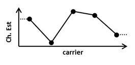
Figure 25: Channel Estimation over Frequency
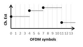
Figure 26: Channel Estimation over Time
The second channel estimation is based on the UERS. These pilots are transferred in each physical resource block (PRB) assigned to the PDSCH addressed to the UE. At this point, there is no knowledge about the PRB allocation. Therefore the channel estimation is done on each PRB. The same resource elements can use multiple UERS, so the averaging over one subframe is used in the time domain to cancel other possible sequences (multi-user interference cancellation). In the frequency domain, linear interpolation is used within the PRBs with zero-order hold applied at the edges.
The channel estimation is delivered sample by sample to the channel equalization modules parallel to the data. The channel equalization determines the result from the data sample d and the channel estimate e by using the following equation:

3.2.3.4 PDCCH Receiver
The PDCCH Receiver works on the output of the CRS-based channel equalization for the first OFDM symbol of each subframe (CFI fixed to 1). It decodes the downlink control information (DCI) for the UE given in the PDCCH channel. The block diagram is shown in Figure 27.
The PDCCH receiver first extracts the PDCCH subcarriers from CRS equalized subcarriers. This is done by evaluating the channel map which is passed to the module in addition to the subcarrier I/Q data. An LLR demapper translates the symbols into soft bits, which are deinterleaved and descrambled by the given system and timing parameters.
After this step, the DCI demultiplexer extracts one DCI message from the PDCCH. The CCE offset parameter can be used to determine the DCI message location. The DCI decoder uses a Viterbi Decoder Core implementation to decode the DCI transport block bits from the given soft bits. The checksum of the cyclic redundancy check (CRC) is calculated on the transport block. If this value matches the configured radio network temporary identifier (RNTI), the message is marked as valid.
The valid DCI message is interpreted according to the implemented DCI format (see Figure 3). A validation module invalidates the DCI message in case the content is not supported, e.g. when MCS > 28. It is also invalidated if a downlink assignment is received outside a downlink subframe.

Figure 27: PDCCH Receiver Block Diagram
3.2.3.5 PDSCH Receiver
Depending on the system configuration, either CRS or UERS equalized QAM symbols are used. The selection is performed inside the PDSCH Sample Select module which is shown in Figure 28. This module selects the incoming subcarrier data after a valid PDSCH Decoding Parameter configuration is received from the PDCCH Decoding. In case of CRS-equalized subcarriers, the first subframe is received before the PDSCH Decoder configuration. In case of UERS-equalized it is received later because of the higher latency of the UERS channel estimation. The PDSCH subcarriers provided by the PDSCH FIFO Control module comprise the PDSCH subcarriers of all 100 resource blocks. Another resource demapper marks the PDSCH QAM symbols as valid or invalid based on the RB allocation from the decoded DCI message which is provided as part of the PDSCH Decoding parameters.
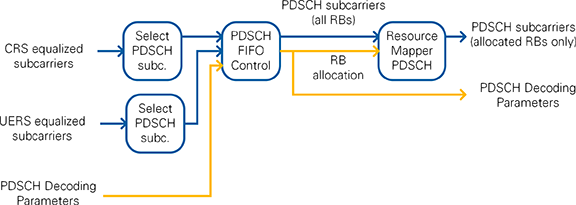
Figure 28: PDSCH Sample Select Block Diagram
The selected PDSCH subcarriers and the corresponding PDSCH Decoding Parameters are passed to the PDSCH Bit Processing module, which is shown in Figure 29.
The valid symbols are interpreted as softbits in the LLR demapper. These softbits are descrambled using the cell parameters and the RNTI. A Scrambler initialization module calculates the initialization value of the shift register which corresponds to 1,600 iterations in just 32 clock cycles.
The PDSCH Transport Blocks are decoded inside the PDSCH Channel Decoder. It includes the LTE PxSCH Channel Decoder described in section 5.3. The necessary parameters (TB size, code block size, number of code blocks) are calculated on the FPGA based on the received DCI message and the configured system settings. The hard bits from the decoder are transferred to the host using a dedicated FIFO. Another FIFO writes the decoding status information to the host.

Figure 29: PDSCH RX Bit Processing Block Diagram
3.2.4 Uplink Transmitter
The Uplink Transmitter is implemented by the FPGA top-level UE. In the block diagrams of Figure 13, it corresponds to the UL TX PHY block.
As shown in the simplified block diagram in Figure 30, the Uplink Transmitter performs the following tasks:
- Physical Uplink Shared Channel (PUSCH) encoding
- Mapping to resource elements (EDSC architecture, see section 5.1.1)
- iFFT conversion + CP conversion (OFDM modulation)
The following reference signals and physical channels are mapped:
- Demodulation Reference Signal (DMRS)
- Sounding Reference Signal (SRS), if enabled
- Physical Uplink Shared Channel (PUSCH)
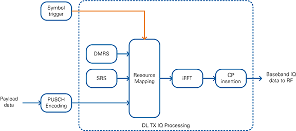
Figure 30: Simplified Block Diagram of Uplink Transmitter
Channel Encoding is performed for the PUSCH as shown in Figure 31. The encoding is performed for each uplink subframe by the FPGA implementation which allows real-time operation. The other signals are read out from look-up tables (LUTs).

Figure 31: Channel Encoding performed in the Uplink Transmitter
3.2.5 Uplink Receiver
The Uplink Receiver is implemented by the FPGA top-level variant eNodeB. As shown in the simplified block diagram in Figure 32, it performs the following tasks:
- CP removal + FFT conversion (OFDM demodulation)
- Demapping of the resource elements to the different physical channels
- DMRS-based channel estimation and equalization
- Physical Uplink Shared Channel (PUSCH) decoding
The following reference signals and physical channels are demapped:
- Demodulation Reference Signal (DMRS)
- Sounding Reference Signal (SRS), if enabled
- Physical Uplink Shared Channel (PUSCH)

Figure 32: Simplified Block Diagram of Downlink Receiver
The uplink receiver (UL RX) receives the I/Q samples in time domain from the RF loop which is derived from the sample streaming project. It performs the I/Q impairments correction, digital down conversion, frequency shift and the down conversion from the ADC sample rate to the LTE sampling frequency of 30.72 MHz.
In contrast to the downlink receiver (DL RX), synchronization is not performed because the UE is required to send the uplink subframe with the correct timing. Therefore, the incoming I/Q samples are already time-aligned.
The demodulation reference signals (DMRS) are used for channel estimation and equalization.
The PUSCH decoder decodes the physical downlink shared channel (PUSCH). The PUSCH configuration parameters are calculated based on the MCS and RB allocation parameters which are set from the host. The decoded PUSCH transport blocks are written to the host using a target-to-host DMA FIFO.
The submodules used for the uplink receiver are very similar to the submodules used for the downlink receiver. Refer to this section for more details about the implementation of these submodules.
3.2.6 Clocking Considerations
There are three main clock domains used inside the FPGA:
- 40 MHz onboard clock
- 120 MHz Sample Clock, 130 MHz Sample Clock, or 200 MHz Sample Clock
- 192 MHz baseband clock
The configuration loops are connected to the 40 MHz clock domain. The configuration information is set prior to execution and used as constants elsewhere in the design.
All LTE baseband processing loops run at a clock rate of 192 MHz. The ADC and DAC interfaces run at the Sample Clock rate, in addition to the sample rate converters that create the 30.72 MS/s I/Q data. The 192 MHz processing clock and Sample Clock are not synchronized, and this difference is accounted for in the design. The processing done in the 192 MHz domain has enough margin to account for frequency tolerances between the 192 MHz clock and the Sample Clock.
The downlink transmitter chain uses a synchronization mechanism to keep the baseband processing aligned and to avoid any underflows or overflows of the FIFO that transfers data between the two clock domains. The Sample Clock domain is used as the absolute time reference. A trigger is generated in the sample clock domain every 10 milliseconds (for each radio frame). This trigger is sent to the 192 MHz processing domain to initiate the creation of a new radio frame. The FIFO between the two clock domains guarantees a constant data rate for the digital up conversion module.
For testing purposes, you can use an internal loopback FIFO on the DL FPGA to bypass the RF by directly transferring samples from the DL TX to the DL RX baseband processing. The internal loopback is disabled by default and can be enabled from the host.
3.3 Host Implementation Overview
The LTE Application Framework provides three sample host implementations which cover all important features of the LTE Application Framework. As described in the section 2.1, three different host implementations are provided:
- Downlink (DL):
- Can be used to establish a downlink link in either a single-device setup or a double-device setup.
- eNodeB:
- Provides the base station (eNodeB) side in a double-device setup.
- Implements the downlink transmitter (DL TX) and the uplink receiver (UL RX) of an eNodeB
- UE:
- Provides the user equipment (UE) side in a double-device setup
- Implements the downlink receiver (DL RX) and the uplink transmitter (UL TX) of a UE
Each host implementation interfaces with the bitfile that was built from the corresponding FPGA implementation. It demonstrates the main functionalities for each implementation. This functionality includes configuration of the FPGA target, exchanging payload data, and monitoring the system status.
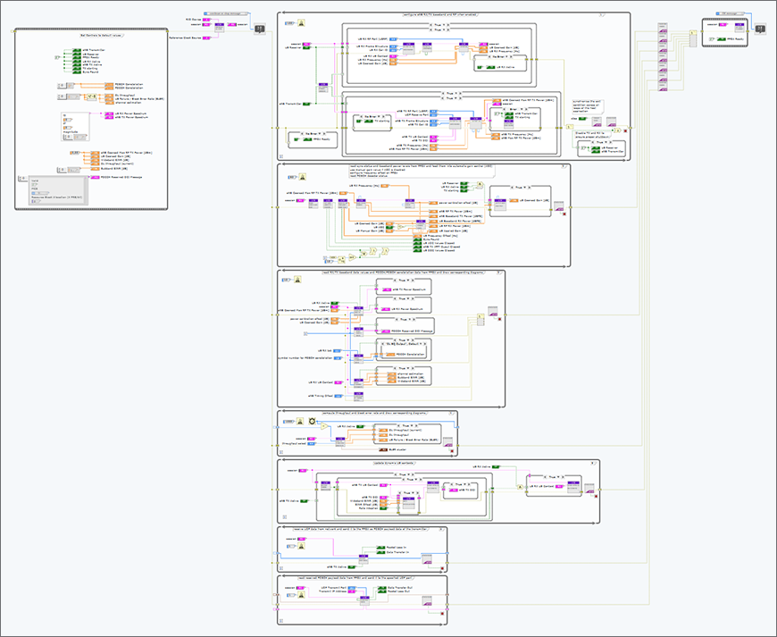
As shown in the schematic overview of Figure 33, each host implementation is split into an Initialization part, several processing loops, and a Cleanup part. Figure 34 shows a screenshot of the LabVIEW G code.
All parts and processing loops are further described in the next sections.
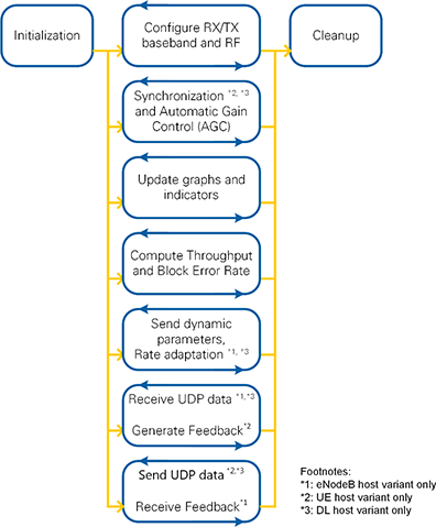
Figure 33: Host block diagram – Schematic Overview
Figure 34 Host Block Diagram – Screenshot of LabVIEW G code
3.3.1 Initialization, Synchronize Exit Condition and Cleanup
The entry point of the code is the initialization block. It sets several controls and indicators to default values. Also, it prepares the session cluster by starting the necessary queues and loading the FPGA bitfile to the configured RIO device. All processing loops use this session cluster during execution to exchange data or to access the FPGA resources.
All processing loops are implemented as while loops which run in parallel during the execution of the host VI. A dedicated stop queue is used to synchronize the stop condition across all loops. The synchronize exit condition loop checks it the Stop button is pressed and accordingly sets the stop condition. The stop condition is also set in case an error occurred in any of the processing loops.
After all processing loops were stopped, the handles from the session are closed, i.e. the queues are stopped and the FPGA reference is closed.
3.3.2 Configure RX/TX Baseband and RF
This loop handles the configuration of the target specific RF and the LTE processing chains. After changes to the RX or TX enable switches, the required parameters are passed to the LTE FPGA processing chain using the settings presented on the front panel, e.g. the Modulation and Coding Scheme (MCS) and the Resource Block Allocation are configured when the downlink transmitter (DL TX) is enabled. After the LTE processing parameters were written to the FPGA, the RF chain is configured and started. Some error cases are caught and presented to the user in dialog boxes.
3.3.3 Synchronization and Automatic Gain Control (AGC)
The loop continuously monitors the received signal power and adjusts the gain for the RX path accordingly. It reports the status of the radio frame synchronization on the FPGA and updates the overflow indicators on the front panel.
This loop also reads the PDSCH decoding status (DL, UE host variants) or the PUSCH decoding status (eNodeB host variant). This information is needed for the outgoing UDP Stream and the throughput calculation. Therefore the elements which are read from the PDSCH/PUSCH decoding status FIFO are duplicated and written to multiple queues.
3.3.4 Update Graphs and Indicators
This loop reads and processes status information from the FPGA and updates the associated graphs and indicators on the host front panel, e.g. it reads the baseband signal of the associated RX or TX processing chain, calculates the power spectra and updates the corresponding graphs. This loop also updates the constellation diagram which is shown on the currently selected tab. For the DL and UE host variant, it also reads the current channel estimation, calculates both the subband and wideband SINR from it and updates the associated graphs and indicators.
3.3.5 Compute Throughput and Block Error Rate
This loop calculates the throughput and the Block Error Rate based on the state of several queues which are filled by the other processing loops.
The queues are emptied on a fixed time basis (1,000 ms) and the elements are accumulated as follows:


where npayload bits is the number of the payload bits per received transport block. This value is the result of the MiniMAC header interpretation.
TBSize is the size of the received transport block. The PDSCH (CRC ok) throughput value considers only the transport blocks which were received successfully (i.e. without CRC errors). The PDSCH (overall) throughput accumulates the sizes of all transport blocks independently on the CRC status.
The sync failure rate, PSyncFailure, and the PDCCH and PDSCH Block Error Rates (BLER) BLERPDCCH and BLERPDCCH are calculated as follows:


Where nSyncSuccessful is the number of times the sync was successful and nSyncChecked is the number the sync status was checked (inside the Synchronization and AGC loop).
nPDCCH is the number of decoded DCI messages, and nPDCCH,CRC ok is the number of messages which were decoded successfully (i.e. without CRC errors).
nPDSCH is the number of decoded PDSCH transport blocks and nPDSCH, CRC ok is the number of PDSCH transport blocks which were decoded successfully (i.e. without CRC errors).
3.3.6 Subframe wise configuration of DL and UL parameters
The system supports a subframe wise configuration of DL and UL parameters in real-time. To use this operation mode, a real-time capable MAC (RT MAC) is needed. This allows the following use cases:
- Scheduling of grants (DL or UL) in real time by the RT MAC and alignment with according data packets
- Support a time-duplex Multi-UE environment, schedule a different UE in each TTI
The message sequence chart of the dynamic DL or UL configuration handling is shown in Figure 35. The FPGA creates a TX timing trigger and provides this trigger to the FPGA and the Host.
- The FPGA starts processing the configuration and data for the current TTI (n) and creates the antenna data for transmission.
- The Host starts preparation of configuration and data for the next TTI (n+1). It writes the dynamic DL or UL configuration and the according data to the FPGA using dedicated H2T DMA FIFOs. The configuration and the data is processed by the FPGA upon receiving the next TX trigger.
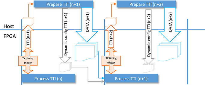
Figure 35: Message sequence chart of dynamic DL (or UL) configuration handling
The downlink and uplink configurations contain the following elements:
- DL TX
- Dynamic DL configuration (cluster)
- RNTI
- Use UERS
- Antenna port
- CCE offset
- DCI message (cluster)
- Dynamic DL configuration (cluster)
- DL RX
- Dynamic DL configuration (cluster)
- RNTI
- Use UERS
- Antenna port
- CCE offset
- Dynamic DL configuration (cluster)
- UL TX and UL RX
- Dynamic UL configuration (cluster)
- RNTI
- SRS configuration (cluster)
- DCI message (cluster)
- Dynamic UL configuration (cluster)
Note that the message sequence chart assumes ideal timing where the total latency from writing the timing indication until reading the Dynamic TX configuration is smaller than 1 ms. This strict regular timing can only be achieved when deploying the host code on a real-time target. When deploying the host code on a Windows operating system, there will be additional jitter which will cause Timing indications to be received too late and as a result the Dynamic DL TX configuration will also be received too late on the FPGA. To compensate for these timing effects, the TTI Handling module has two modes:
- TX RT mode
- True: The TTI handling module assumes that a DL or UL TX configurations is received in time (within one millisecond). If a configuration is missing, an empty configuration will be provided to the CCH/SCH encoding modules.
- False: If no new DL or UL TX configuration is available, the latest valid configuration is used.
- RX RT mode
- True: The TTI handling module assumes that a DL or UL TX configurations is received in time (within one millisecond). If a configuration is missing, an empty configuration will be provided to the CCH/SCH encoding modules.
- False: If no new DL or UL TX configuration is available, the latest valid configuration is used.
By default, TX RT mode and RX RT mode are set to false, which makes the TTI handling module tolerant to missing configuration messages.
The update dynamic UE contexts loop on the host also implements a Rate adaptation functionality which sets the Modulation and Coding Scheme (MCS) depending on the reported wideband SINR value. This value is either read directly from the FPGA (DL host variant) or received from the UE as part of the uplink feedback (eNodeB host variant). The implemented SINR-MCS mapping table is calibrated so that the resulting PDSCH BLER is around 10% if no offset is applied. The control SINR Offset [dB] can be used to apply an SINR offset which allows to achieve a lower PDSCH BLER value.
3.3.7 Receive UDP Data / Generate Feedback
In the eNodeB and DL host variant, this loop handles incoming UDP data, which is used as the payload data for downlink transmission (DL TX). The data is provided by an external application and read from the port number which is specified on the front panel. The data is pushed to the FPGA using a host to target FIFO.
In the UE variant this loop generates the UL feedback message from the received ACK/NACK information and the measured SINR values.
3.3.8 Send UDP Data / Receive Feedback
In the UE and DL host variant, this loop also handles outgoing UDP data. This data stream represents the payload data which was received and successfully decoded from the downlink receiver (DL RX). After the data was transferred to the host using a target to host FIFO, the data is packed into a UDP stream and sent to an external application. The IP address and port number can be specified on the front panel.
In the eNodeB variant this loop receives the UL feedback data and extracts the content to be used in the rate adaptation.
3.3.9 Timing adjustment for multi eNodeB scenarios
In a test scenario with more than 1 eNodeB, you must adjust the timing between the different eNodeBs. For this the parameter Timing Advance is available in the LTE Host UE top-level.
Available parameters in the system:
- LTE Host - eNB Timing Offset for eNB Transmitter
- LTE Host eNodeB - eNB Timing Offset for eNB Receiver
- LTE Host UE - Timing Advance for UE Transmitter
3.3.9.1 DL and eNodeB timing adjustments
The timing offset between RX and TX start is defined by the eNB processing delay and fixed. The trigger point for RX and TX can be adjusted by the parameter eNB Timing offset. The principle is shown in Figure 36.
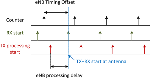
Figure 36: eNB Timing Offset
3.3.9.2 UE timing adjustments
To adjust the TX timing for the UE transmitter, use the Timing Advance parameter. This parameter adjusts the TX start in relation to the synchronized RX. This principle is shown in Figure 37.
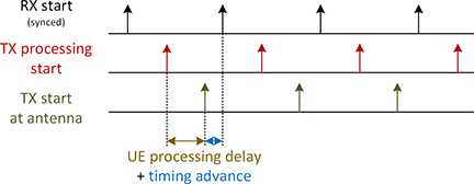
Figure 37: UE timing advance
Conclusion
The LabVIEW Communications LTE Application Framework provides a real-time LTE downlink and uplink, including basic feedback mechanisms running on NI SDR hardware. This framework enables you to focus on a specific area of research by utilizing the existing link and making changes or additions only where desired.
Because of the flexibility of LabVIEW and the modularity of the framework, you can easily exchange portions of the design for prototyping new algorithms for future wireless systems. In addition, LabVIEW's native interface between the host and the FPGA means that the design can be partitioned to profit from the parallel execution on the FPGA as well as calculations on the host.
The FPGA bitfiles shipped with the design are fully functional and support test modes with and without the RF. In addition, you can use external RF equipment, such as the NI 5644R vector signal transceiver, to simulate interference and various channel conditions.
This application framework offers a variety of starting points for wireless research and prototyping.
Questions? Email us at labview.communications@ni.com.
Appendix
5.1.1 EDSC
The enable driven stream combiner (EDSC) combines information from different sources into one stream. You can use the EDSC to map different fields into the frequency domain of one OFDM symbol.
The Stream Generation VI generates control information for the computational VIs. This comprises an enable signal for each computational VI. Only one of these enable signals is asserted at a given time. The asserted enable signal defines the structure of the stream that is generated. Afterwards, an unlimited number of computational VIs provide their data on the output whenever the corresponding enable signal is asserted. When the enable signal is not asserted, the output is zero. Because of this constraint, a simple OR gate can be used to combine the streams.
This design pattern does not use a throttle control mechanism. The computational module can always provide data when the enable signal is asserted. The stream generation ensures that the module can provide data prior to starting.
If the computation of one of the VIs requires pipelining, the other paths between the Stream Generation VI and the OR gate must be delayed to equalize path latencies. Since the output of the computation usually has a wider bit width than the enable signal, add the delay before the computational modules.
5.2 LTE PxSCH Channel Encoder
5.2.1 Functionalities and design considerations
The LTE PxSCH Channel Encoder comprises the following tasks.
Segmentation of incoming bits of shared channel to code blocks and transport blocks as described in 3GPP [2] and [3].
Calculation of code block and transport block CRCs and concatenation of CRCs
Turbo encoding
Rate matching
The module has the following features.
Dedicated for LTE PDSCH / PUSCH
LTE data channel (UL + DL) support only
75 Mbit/s throughput (20 MHz, SISO)
Supports all transport block sizes compliant to 3GPP [3]
Turbo Encoder requires no filler bits
All code blocks of a transport block are equal sized
Supports redundancy version RV=0 only (no HARQ)
Supports UE cat 5 only (no soft buffer limitation in rate matcher)
| Parameter | Value | Comments |
|---|---|---|
| Clock rate in LTE AF | 192MHz | |
| Max. throughput | ≈ 95Mbit/s | LTE 75 Mbit/s support |
| Latency | ≈ 0.8ms | Worst case latency for PRB=100, MCS=28; of minor importance without real time MAC layer |
| FPGA utilization | numbers also include parameter computation for configuration | |
| LUTs | 3333 (1.3%) | Values in () refer to Xilinx Kintex-7 FPGA K410T as used in supported NI USRP and FlexRIO devices |
| Registers | 4093 (0.8%) | |
| Block RAMs (36k) | 3 (0.4%) | |
| DSPs | 12 (0.8%) |
Table 1: LTE PxSCH Channel Encoder facts
5.2.2 Interface
All inputs and outputs offer a 4-Wire handshake interface. The LTE PxSCH Channel Encoder requires a configuration prior to the data. This configuration comprises of the following.
Number of resource elements used for transmission
Modulation (QPSK, 16QAM, 64QAM)
Redundancy version index (0)
Transport block size (Table 7.1.7.2.1-1 of [3])
The incoming data shall be given as Boolean values. The PxSCH Channel Encoder output is also given as Booleans. The mapping from Booleans to symbols is done such that a false equals 1 and true equals -1.
5.2.3 Implementation Overview
The LTE PxSCH Channel Encoder consists of four main modules. Internally, multiple stages parallelize the execution on a code block basis. Each stage can contain a different configuration. The state machines of the modules handshake with each other at the end of the operations to check if computation can continue. If computation cannot continue, the operation of the stages will be stalled. The nomenclature for the data samples on the blue path is based on section 5.1.3 of [2]. The yellow arrows indicate the control information.
In the Configuration Stage, the Parameter Calculation module derives the internal parameters from the given parameter cluster (see section 5.2.1). This calculation is performed once for each transport block.
The internal configuration cluster is consumed by the CRC module. This module calculates the 24-bit CRC checksum for the incoming transport block. Depending on the transport block size, it subsequently segments the transport block into code blocks. If the segmentation results in more than one code block, a 24-bit CRC checksum is calculated for each code block. The CRC checksums are calculated and mapped into the bit stream according to Sections 5.1.1 and 5.1.2 of [2]. The CRC module generates a new configuration out of the given transport block parameters for each code block because all subsequent blocks are working on a code block base.
The uncoded input bits c of each code block are fed into the Turbo Encoder block where the bit stream is duplicated. The first stream is fed directly into a Turbo Encoder, whereas the second copy is fed into an internal interleaver prior to encoding. The output of this interleaver is the bit stream c’. After interleaving, the resulting stream c’ is also encoded using an identical Turbo Encoder as for stream c before. The actual Turbo Encoding algorithm is implemented as defined in Section 5.1.3.2.1 of [2].
The termination of the trellis in the encoder is performed by feeding the bits from the feedback shift registers into the encoder after all information bits are encoded. The resulting termination bits are collected, reordered as defined in Section 5.1.3.2.2 of [2], and mapped into the encoder output streams, forming the d(0), d(1) and d(2) outputs of the encoder. The Encoder block has a separate output for the d(0) stream, while the d(1) and d(2) streams are using the same output port, so that d(0) and d(1) are transferred in parallel in the first chunk of data followed by a second chunk with the remaining d(2) bits. The transfer length of each chunk is based on the code block size K.
The encoder output is written into the circular buffer of the rate matcher. The sub-block interleaving defined in Section 5.1.4.1 of [2] is performed by calculating interleaved write addresses for the circular buffer. When all bits of one code block are written into the circular buffer, the encoding stage is complete and is able to process the next code block. Meanwhile the output stage is able to read out the circular buffer. The readout begins at address k0 and stops after the length of the output sequence reaches E.
5.2.4 Timing
The timings of the different stages of the whole PxSCH Channel Encoder depend on their current configuration. Table 2 lists the processing time in clock cycles for each stage. This list does not take into account the stage handshaking by the state machine.
| Stage | Processing Time [clock cycles] |
|---|---|
| Configuration Stage | 100 |
| Encoding Stage | 14+2*(K+4) |
| Output Stage | E |
Table 2: PxSCH Channel Encoder processing time per stage
The rectangles indicate the valid samples in each stage. The grey rectangle in the upper right corner serves as a scaling reference. The colors indicate the samples of one code block. The configurations belonging to different transport blocks are provided in Table 3.
| Stage | Processing Time [clock cycles] |
|---|---|
| Configuration Stage | 100 |
| Encoding Stage | 14+2*(K+4) |
| Output Stage | E |
Table 3: Configurations for PxSCH Channel Encoder timing figure
Prior to the first transport block (blue), all modules are empty. Therefore, the single code block is passed from one stage to the next right after the stage is finished. At the end of the output stage the resulting bit sequence is available.
The single code block of the next transport block (green) has a lower code rate. Thus, the processing time of the Output Stage is much longer than the processing time of the Encoding Stage. In this case, the reading of the circular buffer of the Rate Matcher during the Output Stage determines the overall throughput. Upon completion of the Output Stage, the Encoding Stage of the next code block (red) is already complete, so the Output Stage of this code block as well as the Encoding Stage of the fourth code block (yellow) can begin immediately.
The third transport block consists of two code blocks (red and yellow). Only one configuration is required for both code blocks. The CRC module segments the input data stream into two successive code block streams and provides a corresponding configuration for each code block.
Due to the high code rate of the last configuration the Output Stage of the first code block (red) is much faster than the Encoding Stage of the next code block (yellow). In this case, the handover to the Output Stage is delayed and the Turbo Encoder limits the throughput of the whole subsystem.
5.2.5 Throughput and Latency
The throughput of the PxSCH Channel Encoder subsystem is limited by the stage with the longest processing time. This could either be the Encoding Stage, the transfer of the encoded data into the circular buffer of the rate matcher, or the Output Stage, depending on the configuration. Based on the assumption that all modules are ready for input data, the throughput can be calculated using the values from Table 2 as processing times (PT). The clock frequency is named fCLK. For the maximum number of resource block,s PRB=100 and the highest format MCS=28 the throughput equals 95.8 Mbit/s at a clock rate of 192 MHz (see also section 5.2.1).
The latency of the complete channel encoding process between the assertion of a valid configuration on the input and the availability of all bits on the Rate Matcher output can be calculated. Additional cycles are required for the stage handshaking, but they are negligible for larger code blocks. For the configuration of 100 PRBs and MCS 28 the latency L is about 0.8 ms.
5.3 LTE PxSCH Channel Decoder
5.3.1 Functionalities and design considerations
The LTE PxSCH Channel Decoder comprises the following tasks as described in 3GPP [2] and [3].
Performs rate matching
Performs turbo decoding
Checks code block and transport block CRCs; concatenates and outputs decoded bits
The channel decoder is fully compliant to the 3GPP LTE standard [2] and [3]. The supported transport block sizes are provided in Table 7.1.7.2.1-1 of [3]. There is no circular buffer limitation (corresponding to UE category 4 or 5 for SISO transmission). Retransmissions are not supported by the LTE Application Framework. Thus, HARQ combining is not included in the channel decoder and the parameter computation is implemented for redundancy version index 0 only. However, the interface lists a currently ignored field for redundancy version already. The signal processing itself is also able to cope with parameter values that result from redundancy version values other than 0.
Dedicated for LTE PDSCH / PUSCH
LTE data channel (UL + DL) support only
75 Mbit/s throughput support (20MHz, SISO)
Support for all transport block sizes compliant to 3GPP [3]
o Turbo decoder requires no filler bits
o All code blocks of a transport block are equal sized
Redundancy version RV=0 support only (no HARQ)
Support for UE cat 5 only (no soft buffer limitation in rate matcher)
| Parameter | Value | Comments |
|---|---|---|
| Clock rate in LTE AF | 192MHz | |
| Maximum throughput | ≈ 95Mbit/s | Depends on number of iterations n of Turbo decoder; LTE 75 Mbit/s support is achieved with n ≤ 4.5 |
| Decode performance: Implementation loss | ≤ 1dB | Depends on configuration of n; largest n providing processing time below 1 ms, required better SNR to achieve a FER=10% compared with an ideal Log-MAP decoder with n → ∞ |
| Latency | ≤ 1.1ms | Worst case latency for n ≤ 4.5; of minor importance without real time MAC layer |
| FPGA utilization | numbers also include parameter computation for configuration | |
| LUTs | 15292 (6.0%) | Values in () refer to Xilinx Kintex-7 FPGA K410T as used in supported NI USRP and FlexRIO devices |
| Registers | 11173 (2.2%) | |
| Block RAMs (36k) | 28 (3.5%) | |
| DSPs | 10 (0.7%) |
Table 4: LTE PxSCH Channel Decoder facts
5.3.2 Interface
All inputs and outputs offer a 4-Wire handshake interface. For its operation the LTE PxSCH Channel Decoder requires a configuration prior to the data. This configuration comprises the following.
Number of resource elements used for transmission
Modulation (QPSK, 16QAM, 64QAM)
Redundancy version index (0), other values are ignored
Transport block size (table 7.1.7.2.1-1 of [3])
The incoming data is given as Log-likelihood Ratios LLR. The quantization of the input LLR also defines the required internal precision of the decoder processing unit. The fewer bits that are spent, the more the performance degrades compared to the floating point model. The best results for precision and resource usage are achieved with 8 bits. The fixed point format is a signed FXP5.3. The LLR input comprises the range from -16 to +15.875 where stronger LLRs have to coerced to the max values. In case of puncturing, a LLR of 0 represents the maximum uncertainty.
The output of the PxSCH Channel Decoder is given as Booleans. The mapping from Booleans to bits is performed such that a False equals 1 and True equals -1.
The number of half-iterations m (in literature it is more common to specify the number of iterations n = m/2) to execute in the Turbo Decoder is configurable at runtime. The value’s fixed-point format of m is an unsigned FXP4.0. For best results regarding decoding performance and throughput, set the number of half-iterations in the range from m = 5 to m = 9. Setting the number of half-iterations m > 9 (n > 4.5) will limit the throughput below 75 Mbit/s at a clock rate of 192 MHz for the decoder.
5.3.3 Implementation Overview
The LTE PxSCH Channel Decoder consists of four main modules. Internally, multiple stages parallelize the execution on a code block basis. Each stage can contain a different configuration. The state machines of the modules handshake with each other at the end of the operations to check if computation can continue., If computation cannot continue, the stages will be stalled. The nomenclature for the data samples on the blue path is based on section 5.1.3 of [2]. The yellow arrows indicate the control information.
In the Configuration Stage, the Parameter Calculation module derives the internal parameters from the given parameter cluster (see section 5.3.2). This calculation is performed once for each transport block.
The internal configuration cluster is consumed by the Rate Matcher. Using a 4-Wire handshake, the weighted softbits e can now be transferred into the circular buffer. The Input Stage is complete when the rate matching output sequence length E is reached. This step is repeated for each code block in the transport block without taking a new configuration. Thus, the configuration cluster contains both values of E according to section 5.1.4.1.2 of [2].
In the Transfer Stage, a reduced configuration is given to the Turbo Decoder. This cluster comprises:
Number of code blocks (C)
Code block size (K)
Last code block flag
After configuration handover, the sequences d(0), d(1), d(2) are read from the circular buffer of the rate matcher and stored into the Turbo Decoder’s Softbit/LLR Input Buffer. Punctured softbits/LLRs are represented by zeros in the sequences. Therefore, no additional puncturing information is needed. This transfer is divided into two chunks. While the sequences d(0) and d(1) are transmitted in parallel in the first chunk, d(2) is transmitted in the second consecutive chunk. The transfer length of each chunk is based on the code block size K.
In the Decoding Stage the Turbo Decoder estimates the encoded bit sequence b in multiple iterations. One full iteration consist of two half-iterations where one half iteration is based on the input sequences d(0) and d(1), whereas the other half-iteration uses an interleaved sequence of d(0) and the received sequence d(2) for estimation of b. During the last half iteration, the bit sequence b is written to the Reordering Buffer. The number of half-iterations m can be changed during runtime.
In the Output Stage the decoded bits are passed to the CRC check module aligned with the configuration cluster. The CRC check module removes and checks the transport block as well as the code blocks CRC checksums. On the output only the bits of sequence a are marked as valid. At the end of the transport block the result of the CRC check is given as control information. There is a Boolean for the result of the transport block check and a cluster of 13 Booleans for the code blocks CRC check where each entry 1 .. C represents one code block.
5.3.4 Rate Matcher details
Rate matching in LTE consists of separate interleaving of the three bit streams from the encoder followed by a circular buffer storing all these bits. The desired code rate is achieved by reading from the circular buffer the amount of bits according to the scheduled resources. This concept allows the theoretical adjustment to any code rate between 0 and 1. If the code rate is higher than the code rate of 1/3 of the encoder, not all bits are read from the circular buffer, whereas in case of smaller code rates, some bits are read more than once.
The rate matcher at the receiver must execute these operations in reverse order. At the beginning the circular buffer is filled with Zeros to easily implement puncturing. Additionally, writing to the circular buffer can be implemented easily as softbit combining by read, add and write back operations. After all received softbits are written to the circular buffer, the three streams are read. Some softbits can still be Zeros, indicating that those bits were not transmitted at all. After deinterleaving, the streams are handed over to the decoder separately.
The Rate Matcher implementation on FPGA consists solely of the circular buffer. The writing to the buffer is in linear order starting at k0 (see section 5.1.4.1.2 of [2]) which is adopted to reflect the leave out of filler bits. It uses read, manipulate and write-back mechanism to enable softbit combining. The following read out of the circular buffer uses special address calculation to reverse the sub-block interleaving (described in section 5.1.4.1.1 of [2]) of the three bit streams d(0), d(1), and d(2) on the fly and provide them in linear order for the decoder.
Additionally, the implementation of the circular buffer does not contain any filler bits unlike the definition in section 5.1.4 of [2]. This has to be regarded for the parameter (e.g. k0) and address calculation as well.
5.3.5 Description of Turbo Decoder implementation
The Turbo Decoder is based on the Max-Log-MAP algorithm also known as the BCJR algorithm and described in Chapter 4 of [4]. The LabVIEW implementation is capable of handling code blocks with a length that is a multiple of eight bits (byte aligned). This condition is fulfilled by all the transport block sizes given in [3].
To achieve the throughput of 75 Mbit/s with up to n = 4.5 iterations (m = 9 half iterations) using a single Turbo Decoder instance, the decoder is internally parallelized with P = 4. Each incoming code block is divided into P = 4 equal length segments of length K / P. Thus, P = 4 identical Max Log MAP decoders estimate the extrinsic information for all code block segments in parallel. Furthermore, the Max Log MAP decoder implementation uses the BCJR algorithm with an additional windowing approximation called next iteration initiation technique to reduce the amount of memory for storage of all internal states.
5.3.5.1 Operation Principle
Three softbit sequences are handed over from the Rate Matcher. These are systematic (S=d(0)) softbits, parity 1 (P1= d(1)) softbits originating from the first convolutional encoder and parity 2 (P2=d(2)) softbits from the second convolutional encoder using an interleaved version of the systematic bits. Internally, the decoder uses two different softbit sets. The first set comprises the received systematic S and parity 1 P1 softbits. The second set consists of the interleaved systematic bits S’ (derived from ) and the parity 2 P2 bits.
The decoding is done iteratively. In each half-iteration the decoder is fed with one set of softbits. Internally the full Trellis diagram is evaluated to search the likeliest way through all states. The a-posteriori output represents the Log-likelihood ratio for each bit. There is also extrinsic information that represents the information gain for each bit from the half-iteration. For the next half-iteration this additional information (called a-priori on the input) is used along with the other set of softbits to refine the estimation. Between half-iterations the extrinsic information must be interleaved or de-interleaved to match the order of softbits (according to the original or QPP interleaved order in the encoder). In the last half-iteration a hard decision is done on the sign of the a-posteriori information to get the decoded bits.
5.3.5.2 Mathematical Operations
Based on the AWGN channel model the probability of encoded bit x can be expressed as exponential term. Because of the Log-likelihood ratios the sum of such terms can be approximated by finding the maximum of the exponents.
For each half-iteration the Trellis diagram for the current code block is set up and evaluated. The first step is the calculation of the state transition probability Gamma (Γ) for each bit (index k) of the code block from the input LLR(yk) (weighted softbits Lcykl) and the a-priori information L(uk). The index l enumerates the elements of the code word (encoded bits). There are two elements in LTE code words of one component encoder (systematic and parity). The previous state is denoted by s’ while the next state is s. The state numbering is based on the encoder’s internal registers. In LTE the encoder has three registers, which translates to eight states. The channel reliability factor Lc is already weighted by the LLR demapper. xkl are the encoded bits created by the encoder during this state transition.
Based on this state transition probability Gamma the forward recursive calculation of Alpha (A) can be performed. Alpha is a vector of probabilities for all eight states of the encoder’s internal registers. This relates to the search of the likeliest path in the Trellis diagram in forward direction. Since the component convolutional encoder in the LTE data channel processing is terminated the start state s is known to be the all zeros state. The start vector A0 therefore exhibits a much higher probability for the zero state than for all other states. Subsequent Alpha vectors Ak are calculated recursively using the Gamma values. The new vector is calculated element by element (Ak(s) for state s).
The backward recursive calculation of Beta (B) starts at the end of the code block. This relates to the search for the likeliest path in the Trellis diagram in reverse order. The end state s is also known to be the all zeros state due to the terminated encoder.
Based on Alpha, Beta, and Gamma the A-Posteriori LLR L(uk|y) for bit index k can be calculated. It uses the Alpha vector Ak-1 corresponding to the accumulated state transition probabilities from the start of the code block up to the previous bit index k-1, with the Beta vector Bk representing the accumulation of future state transition probabilities starting from bit index k up to the end of the code block, and the current Gamma transition probability vector from the received symbol with bit index k. The hard decision for the decoded bit can be derived from the sign of the A-Posteriori result.
As a last step, the Extrinsic information (probability gain from decoding in such a half-iteration) is calculated based on the A-Posteriori values. By subtracting the A-Priori information and the influence of the transmitted softbit estimation, only the information gain is preserved.
5.3.5.3 Parallelization
In order to execute multiple iterations to increase the performance of the Turbo Decoder and improve the overall system sensitivity, the decoding operation must be parallelized to meet the throughput requirements from section 5.3.1.
The Turbo Decoder uses code block segmentation and windowing to reduce the execution time. The size of any code block in LTE is a multiple of eight bits. Therefore it is always possible to split the execution in P = 4 equal length subsegments which are processed in parallel. P = 4 was chosen as tradeoff between achievable throughput or maximum number of half iterations and required resource utilization. For each subsegment there is a separate BCJR Subsegment Decoder instance needed, according to 5.3.5.2.
The subsegments are further split into smaller windows of 32 bit indices. If the subsegment size is not multiple of 32, the first window (window 0) can be smaller in size. The window count w is limited to 48 for the largest code block size. The purpose of this split is primarily to reduce the amount of memory need to store all internal state information, and also to reduce decoding latency from a maximum of K/4 to 32. Instead of complete execution of backward Beta and forward Alpha computation for all K/4 bits before starting A-Posteriori computation, decoding is started at least every 32 bits.
For each half-iteration, Gamma and Beta calculation are started on a subsegment basis. As soon as the Beta vector for the last code bit of one window is available, Alpha computation is triggered. Gamma and Beta values are preserved for each code bit in a LIFO to reverse their ordering and enable calculation of the A-Posteriori values in combination with the Alpha computation output.
Both segmentation and windowing split the underlying Trellis diagram into multiple parts. Because of the termination of the encoder, only the probabilities of the very first and the very last state of the code block Trellis are fixed prior to decoding. For all intermediate subsegments and window cutting edges, the state probabilities are unknown. All the state probabilities are equally set to zero to express this uncertainty.
For the next half-iteration on the same set of softbit inputs (the over next half-iteration) the probability vectors Alpha and Beta of all end states of predecessor subsegments and windows are used as the improved starting values for the successor subsegments and windows. This reflects the actual continuity of the Trellis.
These transitions do not work for consecutive half-iterations because even and odd half-iterations are based on different softbit input sets. The difference originates from the interleaving of the systematic bits for the second component encoder. Thus the order of bits is not the same, which leads to different Alpha / Beta state probabilities. The transition of probability vectors at the cutting edges leads to a completion of the Trellis diagram after a certain number of half-iterations.
5.3.5.4 FPGA Implementation
As described in previous sections, the Turbo Decoder covers multiple operation stages. The handshaking between the stages and the control signal for each half-iteration are generated in a state machine not shown in the block diagram.
At the end of the Transfer Stage, the systematic bits and parity bits are available in the Softbit Input Buffer. This double buffer supports the independent operation between the Transfer and Decoding stage. The systematic bits are stored in linear (S) order as well as in interleaved order (S’) for even and odd half-iterations using two different memories. The encoder termination bits are separated from the incoming data streams by the Termination Bit Extraction module and stored in the Termination Bit Memory.
Upon startup of the Decoding Stage operation, the termination bits are read from the Termination Bit Memory into the Initial Beta Calculation module. They are used to determine the start values of the Beta probability vectors for the first and the second set of softbits. Both vectors are saved to the Stake Memory that handles the state transitions described in section 5.3.5.3 between subsegments and windows.
Upon completion of the initial Beta calculation, the first half-iteration is triggered. Four parallel streams are read from the A-Priori and Softbit Buffer to feed the four BCJR Subsegment Decoder instances within the BCJR decoder module. The start states of Alpha and Beta are provided in parallel by the Stake Memory. At the end of each subsegment window the probability vectors are written back to that memory. The memory uses double buffering to store two different sets of state vectors assigned to the different sets of softbits (S & P1 or S’ & P2).
The A-Posteriori and Extrinsic outputs of the BCJR decoder provide four elements per clock cycle from the four subsegment decoders. The QPP Reordering module assigns addresses to each element and reorders the four streams corresponding to the QPP interleaving in the encoding process. The operation mode toggles between interleaving and deinterleaving for even and odd half-iterations, respectively, to always enable linear read-out of the A-Priori buffer. Double buffering is used to allow read and write operations simultaneously.
During the last half-iteration, hard decision of the A-Posteriori values is done inside the QPP Reordering module, and the Boolean data is written to the Bit Reordering Buffer.
In the Output Stage, the decoded bits are read from the Bit Reordering Buffer using a 4-Wire handshake to throttle the output based on the downstream modules. Due to the implemented double buffering, the decoding of the next code block can already begin.
5.3.6 Timing of the PxSCH Channel Decoder
The timings of the different stages of the whole PxSCH Channel Decoder depend on their current configuration. Table 5 lists the processing time in clock cycles for each stage. This list does not take into account the stage handshaking by the state machine.
| Stage | Processing Time [clock cycles] |
|---|---|
| Configuration Stage | 100 |
| Input Stage | E |
| Transfer Stage | 10+2*(K+4) |
| Decoding Stage | 19+(K/4+24+min(32, K mod 128))*(number of half-iterations) |
| Output Stage | 1+K |
Table 5: PxSCH Channel Decoder processing time per stage
The rectangles indicate the valid samples in each stage. The grey rectangle in the upper right corner serves as a scaling reference. The colors indicate the samples of one code block. The configurations belonging to different transport blocks are given in Table 6.
| Color | Number of PRBs | MCS | E | C | K |
|---|---|---|---|---|---|
| Blue | 20 | 9 | 5760 | 1 | 3136 |
| Green | 20 | 10 | 11520 | 1 | 3136 |
| Red / Yellow | 12 | 28 | 3456 | 2 | 4416 |
Table 6: Configurations for PxSCH Channel Decoder timing figure
Prior to the first transport block (blue), all modules are empty. Therefore, the single code block is passed from one stage to the next immediately after the stage is finished. At the end of the output stage the transport block (TB) CRC is removed and the resulting bit sequence is available.
The single code block of the next transport block (green) has a lower code rate. Thus the processing time of the Input Stage is much longer than the processing time of the Transfer Stage. In this case the writing of the circular buffer of the Rate Matcher during the Input Stage determines the overall throughput. Upon completion of the Input Stage the previous code block (blue) is already in the Decoding stage. Thus, the Transfer Stage for the code block can begin immediately and fill the second page of the Turbo Decoder’s softbit buffer. This consecutive execution continues up to the output since the code block sizes of the first two transport blocks are equal.
The third transport block consists of two code blocks (red and yellow). Only one configuration is needed for both code blocks. The Rate Matcher ensures that the softbits on the input are taken code block by code block. The configuration is asserted close to the completion of the Input Stage of the code block of the second transport block (green), but it can be asserted anytime during the previous Input Stage(s).
Due to the high code rate of the last configuration, the Input Stage of the first code block (red) is much faster than the Transfer Stage of the previous code block (green). In this case the Input Stage is stalled until the previous code block enters the Decoding Stage. This occurs for the second code block (yellow) as well. The processing time of the Decoding Stage is a few clock cycles longer than the Transfer Stage for this configuration. Upon completion of the Transfer Stage for the second code block (yellow), the handover to the Decoding Stage is delayed as well. In both cases the Turbo Decoder limits the throughput of the whole subsystem.
After the last code block of a multi code block transport block has been processed by the Output Stage, the transport block CRC and all code block CRCs are available.
5.3.7 Throughput and Latency
The PxSCH Channel Decoder subsystem throughput is limited by the stage with the longest processing time. This depends on configuration, especially the code rate. Based on the assumption that all modules are ready for input data, the throughput can be calculated using the values from Table 5 as processing times (PT). The clock frequency is named fCLK. For the maximum of 100 PRBs and the highest MCS 28 with the number of half iterations set to m = 9, the throughput reaches about 82 Mbit/s at a clock rate of 192 MHz. This number still outreaches the requirement from 5.3.1.
The latency of the complete channel decoding process between the assertion of a valid configuration on the input and the availability of the CRC result(s) on the output can be calculated. Additional cycles are needed for the stage handshaking, but they are negligible for larger code blocks. For the configuration of 100 PRBs, MCS 28, and m = 8 half-iterations, the latency L is about 0.94 ms. This value is sufficient to connect the decoding core with a real-time MAC.
5.4 Viterbi
The control channel, called PDCCH in LTE, is protected with a convolutional code against transmission errors. The corresponding receiver uses a Viterbi decoder implementing the Maximum Likelihood Sequence Estimation (MLSE) algorithm based on softbit input. Convolutional codes with a constraint length of 7 are used. Thus there is a 64-state Trellis. Other parameters of the convolutional code are summarized in Table 7.
| Operation Mode | LTE |
| Code rate | 1/3 |
| Code polynomials | [133, 171, 165] |
| Termination | Tail-biting |
Table 7: Parameters of the convolutional encoder
5.4.1 Design considerations
The LTE PDCCH has a maximum code block length of 70 bits (for DCI format 2C using 20 MHz bandwidth as defined in section 5.3.3.1.5C of [2]). Currently the code block length in the LTE Application Framework is fixed to 48 bits including CRC. This code block is received once every TTI of 1 ms. The signal processing in the LTE Application Framework runs at a clock rate of 192 MHz.
5.4.2 Operation Principle
The Viterbi decoder consists of the three modules: branch metric computation, path metric accumulation and survivor selection, and traceback handling for actual decoding.
In the branch metric computation, the received softbits are multiplied by the hypothesis to form the state transition metric. This branch metric updates the path metric of all 64 states and calculate the surviving path. The corresponding Boolean bit value is stored in the traceback memory. After a certain number of iterations, the maximum path metric is determined, and from its state the traceback memory is evaluated backward to decode bits in history along the most likely path in the Trellis.
The metric computation runs in streaming mode and fills the traceback buffer continuously, but the actual decoding with evaluation of the traceback memory is initiated only every traceback length time instances. Thus you must flush the metric computation with artificial softbits to enable traceback evaluation and decoding for the last bits of a code block as well.
5.4.3 Interface
The Viterbi core can handle one bit per clock cycle. Handshaking is implemented in the direction of upstream and downstream modules. All modules must be able to handle continuous data streaming. The input valid and output valid signals are used to indicate valid samples.
Aligned to the data is a data bit? flag. This Boolean is not used by the core but delays parallel to the processing. It can be used to distinguish data bits and flushing bits, which are required to decode the last bits of the code block.
The incoming data is given as Log-likelihood Ratios. Based on the code rate, 2 or 3 code bit inputs must be used. The fixed-point format is FXP4.1. Based on the quotient a strong probability for a positive transmitted symbol uk is mapped to 7.5. The strong probability towards a negative transmitted symbol uk is mapped to -8. In case of puncturing, zero represents the maximum uncertainty.
The output of decoded bits is given as a Boolean. The mapping from Booleans to symbols is performed such that a False equals 1 and True equals -1.
The operation mode and the traceback length must be constant. The traceback length defines the minimum number of states the Trellis is continued before decoding the current state. The valid range is 1 to 127.
5.4.4 Implementation
The branch metric computation is implemented with simple sign changes and additions. For LTE, three softbits build the input and are used to compute the 8 different branch metric values. This reflects the code rate of 1/3 of the encoder.
Both Application Frameworks use only one implementation of the path metric computation, often named Add-Compare-Select in literature. For each of the 64 states, the path metric values of the two preceding states are updated with the corresponding branch metrics. The larger of the resulting values is stored as the new path metric for this state. At the same time, the result of the comparison is stored as a Boolean value to mark the more likely state transition of the surviving path. The outputs of the submodule are a new 64 element vector of path metrics and a 64 element Boolean vector of survivor paths for every bit vector input.
In LTE, tail-biting is used, and at the receiver no information about the start state is available. Hence the best path metric start vector has equal values for all states.
The path metric computation submodule does not have a reset. Thus, at the end of a code block, the path metric memory must be similar to the described start vector to allow continuity of code block handling. This is achieved by flushing appropriate softbits (see section 5.4.2). For the tail-biting convolutional coding in LTE, all path metric values should be the same at the start of a code block. This is achieved by flushing softbits with the value 0, representing complete uncertainty.
Normalization of the path metric values is used to avoid infinitively growing values and restrict the bitwidth. Since only the difference between path metrics is of interest, but not their absolute value, normalization does not influence the decoding result. The process occurs over two clock cycles. In the first clock cycle, all path metric values are checked against a threshold before they are written to memory. In the second clock cycle dependent on the threshold comparison, a constant value is subtracted from the branch metric prior to updating the path metrics.
The survivor path is written to two traceback memories. After traceback length samples one of the two traceback paths is triggered. The most probable state at this point in time is the one with the largest path metric value. Its index is provided by the Find Best State module. Starting from this state, the Traceback Calculation module recursively calculates the previous state based on the survivor path vectors from the traceback memory. The decoded bit is derived from the LSB of this survivor state.
Because the first decoded bits of the survivor path show lower reliability than later elements in the traceback, the first half of the bits is discarded. The order of the remaining decoded bits must be reversed because the traceback memory is evaluated backwards. Both operations are performed in the Bit Reordering module.
As a last step, the outputs of the two traceback chains are combined to a final decoded sequence that is available on the output.
5.4.5 Timing
Timing is independent of the chosen operation mode, but depends on the traceback length. As described in section 5.4.4 there are two traceback chains which are illustrated in different colors. The horizontal axis represents the time. For reference, a scale with multiples of traceback length clock cycles is visible on the top. The timing diagram assumes that there is a valid input in each clock cycle. The traceback memory is empty at the beginning.
All input data is processed in the branch and path metric calculation. This adds two cycles of latency before storing the data to the traceback memory. The first traceback memory is read as soon as two times traceback samples are written. The second traceback chain starts another traceback samples delay. The Traceback Calculation module adds one cycle of latency. At the output of the Bit Reordering module, only the second half of the samples is declared valid after two times traceback length elements have been written. The output of both traceback chains is combined to a continuous output stream.
If the input is not valid, each clock cycle the input pattern is kept until the traceback memory input. Afterwards, the traceback decoding and bit reordering are performed burst-wise. In this case, the latency every wait cycle on the input increases the latency for the first code block input by one cycle. NI recommends that you flush the Viterbi core with a continuous stream to have the minimum latency for the end of the code block.
This concept results in a decoding latency of four times the traceback length (plus 13 clock cycles processing time) because during two times the traceback length, the traceback buffer is written and during another two traceback lengths evaluation and decoding takes place. The evaluation in chunks of two times the traceback length makes it necessary to flush the Viterbi decoder with exactly the same number of input softbit triples.
5.4.6 Resource Usage
The Viterbi implementation occupies the FPGA resources listed in Table 8.
| Operation mode | LTE |
| LUTs | 4236 |
| Registers | 2018 |
| Block Ram (36k) | 2 |
Table 8: Viterbi resource usage
5.4.7 Performance
5.4.7.1 Throughput
The throughput in MS/s is equal to the clock rate in MHz since the core is capable of handling one sample each clock cycle. Synthesis of the core is successful up to a clock rate of 300 MHz.
Abbreviations
| Abbreviation | Meaning |
|---|---|
| 3GPP | 3rd Generation Partnership Projects |
| ACK | Acknowledgement |
| ADC | Analog Digital Converter |
| AGC | Automatic Gain Control |
| BLER | Block Error Rate |
| BW | Bandwidth |
| CCE | Control Channel Element |
| CFI | Control Format Indicator |
| CRC | Cyclic Redundancy Check |
| CRS | Cell Specific Reference Symbols |
| CW | Continuous Wave |
| DAC | Digital Analog Converter |
| DCI | Downlink Control Information |
| DL | Downlink |
| DMRS | Demodulation Reference Signal |
| eNB / eNodeB | Evolved NodeB (base station in LTE network) |
| FAM | Frontend Adapter Module (RF module) |
| NACK | Negative Acknowledgement |
| MAC | Medium Access Control Layer |
| MCS | Modulation and Coding Scheme |
| MLSE | Maximum Likelihood Sequence Estimation |
| OFDM | Orthogonal Frequency-Division Multiplexing |
| PBCH | Physical Broadcast Channel |
| PCFICH | Physical Control Format Indicator Channel |
| PDCCH | Physical Downlink Control Channel |
| PDSCH | Physical Downlink Shared Channel |
| PDU | Protocol Data Unit |
| PHICH | Physical Hybrid-ARQ Indicator Channel |
| PHY | Physical Layer |
| PLCP | PHY Layer Convergence Protocol |
| PN | Pseudo Noise |
| PRB | Physical Resource Block |
| PSS | Primary Synchronization Sequence |
| PUCCH | Physical Uplink Control Channel |
| PUSCH | Physical Uplink Shared Channel |
| QAM | Quadrature Amplitude Modulation |
| RF | Radio Frequency |
| RX | Receive |
| SDL | Specification and Description Language |
| SDU | Service Data Unit |
| SINR | Signal to Interference Noise Ratio |
| SISO | Single Input Single Output |
| SRS | Sounding Reference Symbols |
| SSS | Secondary Synchronization Sequence |
| TB | Transport Block |
| TDD | Time Division Duplex |
| TX | Transmit |
| UDP | User Datagram Protocol |
| UE | User Equipment (user device in LTE network) |
| UERS | UE Specific Reference Symbols |
| UL | Uplink |
Bibliography
3GPP, TS36.211: Evolved Universal Terrestrial Radio Access (E-UTRA); Physical Channels and Modulation (Release 10), V10.7.0, 2013-02. | |
3GPP, TS36.212: Evolved Universal Terrestrial Radio Access (E-UTRA); Multiplexing and channel coding (Release 10), V10.8.0, 2013-06. | |
3GPP, TS36.213: Evolved Universal Terrestrial Radio Access (E-UTRA); Physical layer procedures (Release 10), V10.12.0, 2014-03. | |
L. Hanzo, T. H. Liew, B. Yeap, R. Y. S. Tee and S. X. Ny, Turbo Coding, Turbo Equalization and Space-Time Coding, 2011. |

