LabVIEW Communications 802.11 Application Framework 2.0 and 2.0.1
Overview
2.3 Compliance to IEEE 802.11 Standard
3.1 Interface between MAC and PHY
3.2 Partitioning between FPGA and Host
7.3 Viterbi Decoder Implementation
1 Intro
The 802.11 Application Framework provides a ready-to-run, easily modifiable real-time physical layer (PHY) and lower medium access control (MAC)-layer reference design based on the 802.11 wireless standard. The 802.11 Application Framework is available with the LabVIEW Communications System Design Suite, also referred to as LabVIEW Communications.
This application framework provides a substantial starting point for researchers looking for ways to improve the 802.11 standard by exploring brand-new algorithms and architectures that can support the tremendous increase of the number of terminals, inventing new waveforms by which to modulate and demodulate the signals, or finding new multi-antenna architectures that fully exploit the degrees of freedom in the wireless medium.
The 802.11 application framework is comprised of modular PHY and MAC blocks implemented using LabVIEW Communications. It is designed to run on the powerful Xilinx Kintex-7 FPGA and an Intel x64 general-purpose processor, which are tightly integrated with the RF and analog front ends of the NI software defined radio (SDR) hardware.
The framework is designed from the ground up for easy modifiability, while adhering to the main specifications of the 802.11 standard. This design allows wireless researchers to quickly get their real-time prototyping laboratory set up and running based on the 802.11 standard. They can then primarily focus on selected aspects of the protocol that they wish to improve, and easily modify the design and compare their innovations with the existing standards.
2 Scope
The 802.11 Application Framework provides functional elements of the physical (PHY) as well as the MAC layer of a single station. This code includes receiver (RX) and transmitter (TX) functionality and functional elements for channel state handling, slot timing management, and backoff procedure handling.
The following subsections describe which PHY and MAC functionalities from the 802.11a and 802.11ac standards are supported by the 802.11 Application Framework version 2.0 and 2.0.1, as well as the compliance to the 802.11 standards [1] and [2].
2.1 PHY Layer
The 802.11 Application Framework provides the following PHY transmitter functionalities:
- Scrambler
- Convolutional coding and bit interleaving
- BPSK/QAM constellation mapper up to 256-QAM
- Pilot sequence generation
- Signal fields generation
- OFDM symbol generation based on IFFT
- Guard interval (GI) insertion
- Addition of training fields
Corresponding functionalities, supplemented by specific functions, are provided for the receiver side:
- Clear channel assessment (CCA) based on energy detection as well as on signal detection
- Packet detection
- Automatic gain control (AGC)
- Time and frequency synchronization
- Guard interval removal
- OFDM symbol demodulation based on FFT
- Channel estimation and zero-forcing equalization
- BPSK/QAM demodulation
- Deinterleaving
- Convolutional decoding based on Viterbi decoding
- Descrambling
- Signal fields decoding and reconfiguring the receiver based on signal fields information
Notice that the terms guard interval and cyclic prefix are used synonymously in this document.
The 802.11 Application Framework is designed to support different OFDM configurations as specified in Chapter 18 of [1] and Chapter 22 of [2]. In version 2.0 and 2.0.1 of the Application Framework, the 20 MHz 802.11a and 20 MHz (VHT20) and 40 MHz (VHT40) channel widths from 802.11ac are supported 1.
The 802.11 Application Framework follows the PHY frame format as specified in Section 18.3 of [1] for 802.11a and in Section 22.3 of [2] for 802.11ac. Figure 1 and Figure 2 show the formats for 802.11a and 802.11ac, respectively. Fields specifically needed for the 802.11ac format have the name extension Very High Throughput (VHT), and fields specifically needed for the 802.11a format are referred to as Legacy.
Figure 1: PHY frame format 802.11a
Figure 2: PHY frame format 802.11ac
Depending on the subcarrier format, the PHY frame consists of the following fields:
- Legacy short training field (L-STF), a static field that is used for packet detection and AGC at the receiver.
- Legacy long training field (L-LTF), a static field that is used for time and frequency synchronization as well as channel estimation.
- Legacy signal field (L-SIG), a dynamic field that contains information about the applied modulation and coding scheme (MCS) and the frame length.
- VHT signal field A (VHT-SIG-A), a dynamic field that contains information about the applied channel bandwidth, MCS, and, if configured on MIMO, multi-user settings.
- VHT short training field (VHT-STF), a static field to be used for improving AGC estimation when performing MIMO transmission.
- VHT long training field (VHT-LTF), a static field to be used for MIMO channel estimation purposes.
- VHT signal field B (VHT-SIG-B), a dynamic field containing information of the frame length and the MCS for single-user or multi-user modes.
- Legacy or VHT data (L-DATA or VHT-DATA) is a dynamic field, which is uniquely defined by the MAC message. The number of OFDM symbols NSYM used for the data depends on the chosen MCS and the payload length.
The number of OFDM symbols necessary for the demodulation of the PPDU data or for channel estimation during a null data packet (NDP) 2 in the VHT-LTF field per frame can be either 1, 2, 4, 6, or 8. The number of OFDM symbols is determined by the total number of space-time streams across all users being transmitted in the VHT PPDU 2.
2.2 MAC Layer
The 802.11 Application Framework provides the following MAC transmitter functional elements:
- MPDU generation for ACK frames and data frames
- Support of A-MPDU generation with a single MPDU as in Section 8.6.1 of [1]
- Slot timing management
- Backoff procedure
- Frame check sequence (FCS) generation.
Corresponding functional elements are provided for the receiver side:
- FCS check
- Address check and frame type handling including triggering of ACK frame transmission
- MAC service data unit (SDU) extraction
- Channel state handling
These functional elements listed in the preceding list allow the following capabilities as defined in Section 9.3 of [1]:
- Basic distributed coordinate function (DCF)2
- Transmission and reception of DATA-ACK frame sequences with SIFS timing
This MAC functionality is implemented on the FPGA and tightly integrated with the PHY to fulfill the requirements for interframe spacing, such as SIFS, DIFS and EIFS, as well as slot timing management to allow frame exchange sequences, such as DATA-ACK and basic DCF for carrier sense multiple access with collision avoidance (CSMA/CA). Therefore, this functionality is referred to as lower MAC throughout the document.
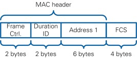
The 802.11 Application Framework follows the frame structure for the MPDU as defined in Section 8 of [1]. Figure 3 and Figure 4 show the packet structure used for data and ACK frames, respectively.
Figure 3: Structure of a MAC data frame
Figure 4: Structure of a MAC ACK frame
A MAC frame consists of the MAC header, the frame body, which may not be present in some frames, and the FCS field.
The MAC header consists of the following elements:
- Frame control
- MAC data frame: Type: Data, Subtype: Data
- MAC ACK frame: Type: Control, Subtype: ACK
- Duration ID: Empty, filled with Zeros
- Address 1: Destination MAC address
- Address 2: Source MAC address
- Address 3: Empty, filled with Zeros
- Sequence Control: Fragment Nr.: 0, Sequence Nr.: 0...4095
- Address 4: Empty, filled with Zeros
- MAC header can be extended to include the fields QoS Control and HT Control. These fields are not implemented in version 2.0 and 2.0.1.
- The frame body consists of MSDU.
- The FCS consists of a 32-bit CRC as defined in Section 8.2.4.8 of [1].
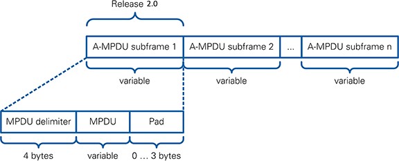
Figure 5 shows the A-MPDU format and also indicates that the 802.11 Application Framework version 2.0 and 2.0.1 supports A-MPDU with one single MPDU as in Section 8.6.1 of [1].
Figure 5: Format of A-MPDU
2.3 Compliance to IEEE 802.11 Standard
The 802.11 Application Framework is designed to be compliant to the IEEE 802.11 specifications. To keep the design easily modifiable, the 802.11 Application Framework focuses on the core functionality of the IEEE 802.11 standard.
Besides the standards-compliant implementation of the functionality mentioned in Section 2.1 and 2.2, the 802.11 Application Framework supports the following features:
- Long guard interval only
- Single input single output (SISO) architecture, ready for MIMO
- Support of single user only for 802.11ac applications
- VHT20 and VHT40 for 802.11ac applications
- A-MPDU with a single MPDU for 802.11ac applications
- Initial transmissions only, architecture ready for retransmissions
- The backoff value is fixed on the FPGA but configurable during run-time using the host interface
The 802.11 Application Framework deviates in the following ways from the IEEE 802.11 specifications:
For immediate access to the medium, the medium is sensed not for the DIFS period of 34 ms, but it is sensed for 9 ms x backoff. Because of that condition, the default backoff has been set to 4. For more information about this subject, contact the NI support team.
2.4 Graphic Formatting
Throughout this document, graphic elements are formatted as described in Table 1.
| Element | Usage |
| Blue rectangle (rounded edges) | Code block or VI |
| Blue rectangle | Code entity |
| Blue arrow | Data path |
| Yellow arrow | Control path |
| Red arrow | Reference to element |
Table 1: Formatting Used for Graphics
3 Architectural Overview
This section provides an overview of the 802.11 Application Framework architecture. Section 3.1 provides information about the basic design ideas and their implications for the partitioning between the FPGA and the host. Section 3.3 gives an overview about design considerations, such as 802.11-specific timing requirements, clocking concepts, and the level plan.
3.1 Interface between MAC and PHY
As the Application Framework targets a wide range of researchers, the design is as close as possible to the IEEE 802.11 specifications.
An implication of this design is that the interface between PHY and MAC follows the PHY_SAP interface as described in Section 4.9 of [1]. Moreover, the Application Framework also follows the concept of PHY service primitives as described in Section 18 of [1] and Section 22 of [2]. For the sake of simplicity, the content of those PHY service primitives is aligned with the implemented feature set.
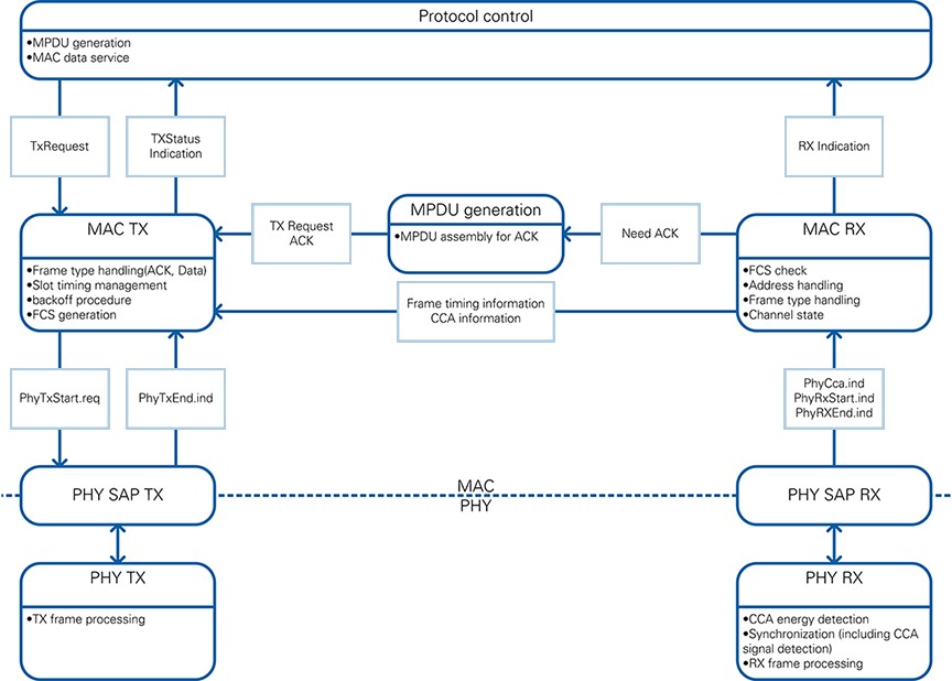
Figure 6 shows the partitioning within the PHY and lower MAC, which is very close to the proposed concept of the IEEE 802.11 SDL specifications. Refer to Section J.5 of [1] for more information about the SDL specifications. The tight timing requirements required modifying the concepts from the 802.11 specifications to fit to the hardware platform. For example, the MPDU generation module is connected to MAC RX and MAC TX directly, which is used for accelerated MPDU assembly that is needed for the ACK frame generation.
Figure 6: Functional split between PHY and lower MAC
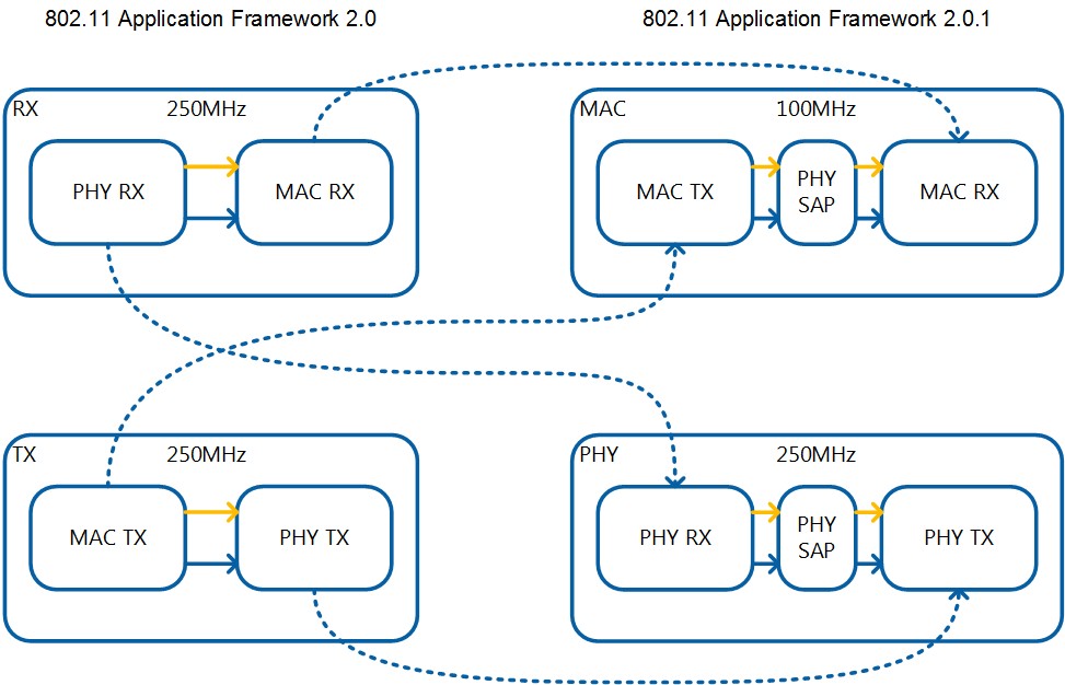
Up to version 2.0 the 802.11 Application Framework is divided into two loops for RX and TX processing respectively. This design was easy to understand but had some disadvantages when it came to extensions in the lower MAC. Whereas the PHY needs to run at 250 MHz to meet SIFS timing constraints the MAC only needs a clock speed of an eighth of the PHY as the MAC processes data bytewise and the PHY bitwise. There is only a small overhead of data exchange between PHY and MAC in 2.0 for information exchange about ACK transmission.
Starting with 2.0.1 the partitioning of the FPGA changes, as shown in Figure 7. RX and TX PHY still run at 250 MHz in a single loop. The MAC RX and TX moved to a new loop which runs at 100 MHz clock speed which is sufficient for MAC data processing3. The reduced clock speed relaxes timing constraints for the MAC at lot making it easier to extend its functionality on the FPGA. The new partitioning requires more data exchange between the loop which also has to take clock crossing into account. Therefore all events between MAC and PHY are exchanged via handshakes. The PSDU data between MAC and PHY is transferred with a FIFO on both RX and TX.
Figure 7: MAC and PHY loops in version 2.0 and version 2.0.1
The 802.11 Application Framework version 2.0 and 2.0.1 provide a subset of upper MAC functionality only. Since just a limited set of frame types is supported and no retransmissions functionality is implemented, the protocol control function, which is considered part of the upper MAC, is quite simple. However, the design can be extended to include more functionality, as the interfaces between the layers and the FPGA and host are already available and can be scaled towards more functionality.
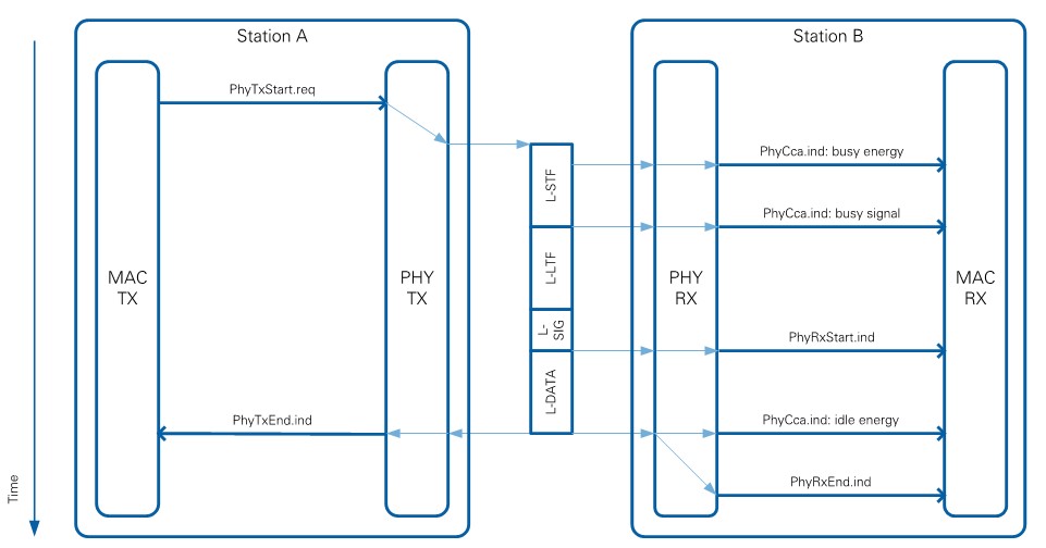
An example for the sequential order of PHY service primitives for regular transmission and reception is shown in Figure 8. For version 2.0 and 2.0.1 of the Application Framework, only primitives that are essentially needed are implemented. An example for a primitive that is not implemented is the PhyTxStart.cnf, which could indicate an error event from PHY to MAC after a PhyTxStart.req is received by the PHY layer.
Figure 8: PHY service primitive sequence chart for regular RX and TX
3.2 Partitioning between FPGA and Host
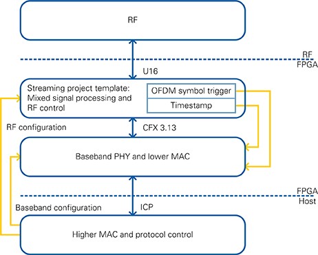
The functionality as described in Chapter 2 and the architectural split described in Section 3.1 are mapped to the host processor, target FPGA, and RF hardware as shown in Figure 9.
The target FPGA contains the lower MAC and baseband PHY layer algorithms for both TX and RX. It also contains RF front-end control functionality taken from the sample streaming projects of the supported RF devices and sample rate conversions to interface baseband signals to the RF front end.
The host processor is dedicated for upper MAC layer functionality, including protocol control. For version 2.0 and 2.0.1 of the Application Framework, MPDU generation for data frames is implemented on the FPGA. This implementation might change in upcoming releases after LabVIEW Communications supports real-time operating systems.
The data path interface between the host and target is realized using a proprietary message-based interface communication protocol (ICP), which is described in Section 7.2.2. The control path interface between the host and target for baseband configuration is implemented using LabVIEW controls and indicators. RF configuration is completed using target-specific driver VIs.
Figure 9: Functional split between Host, FPGA and RF
3.3 Design Considerations
3.3.1 Clocking
There are two clock domains within the FPGA design. The first clock domain is for the RF loop. It depends on the target and is referred to as the data clock. For the USRP RIO with 40 MHz bandwidth, data clock is set to 120 MHz. For the USRP RIO with 120 MHz or 160 MHz bandwidth, it is set to 200 MHz. For the FlexRIO design, data clock is set to 130 MHz.
The second clock domain is used for baseband processing. This clock rate has to also fulfill the requirements for 80 MHz bandwidth support. For this purpose, a 256-point FFT must run for each OFDM symbol. The Xilinx FFT is set to Radix-4, Burst I/O architecture to produce a continuous output of this core with minimum latency. With these settings, the FFT requires 871 cycles for loading data, executing, and unloading data, which are executed sequentially. That process leads to a minimum clock rate of 241.94 MHz, assuming an OFDM symbol duration of 3.6 µs with a short guard interval. Please notice that a short guard interval is not implemented in the version 2.0 and 2.0.1 of the 802.11 Application Framework, but the design is prepared for the future use of a short guard interval. Hence, the baseband clock is set to 250 MHz for all targets. Based on this clock rate, the computation of each OFDM symbol of 4 µs duration (with long guard interval) can take up to 1,000 clock cycles.
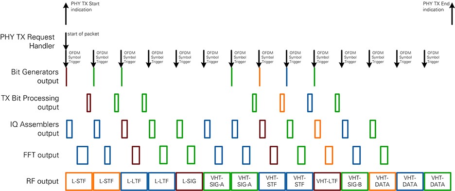
Both clock domains are asynchronous because they do not use the same reference clock. The Application Framework uses FIFOs to transfer data between the RF and the baseband loops. This transfer is straightforward for the RX chain since the samples are taken from RF to the higher rate baseband loop as soon as they are available. The TX chain produces a large number of samples per packet. This large number of samples could lead to overflows when transferring data to the RF loop, which has a fixed sample rate of 80 MS/s. To avoid overflows, the Application Framework generates the TX samples OFDM symbol-wise, and a trigger is generated in the RF clock domain. This architecture means that the FIFO fills at the same rate as it is read from.
3.3.2 Timing Constraints
To ensure efficient use of the shared unlicensed spectrum, the 802.11 standard defines challenging requirements for the interframe timing, in particular for the frame transmissions after a frame reception and for the frame transmissions after channel sensing. To meet those requirements, tight integration of PHY and lower MAC functionalities is needed. In this subsection, the requirements of the 802.11 specifications for systems with OFDM-based PHY layer are described and the values assumed in the 802.11 specifications are compared to actual achieved values of the 802.11 Application Framework.
3.3.2.1 Timing Budget for Transmission after Frame Reception
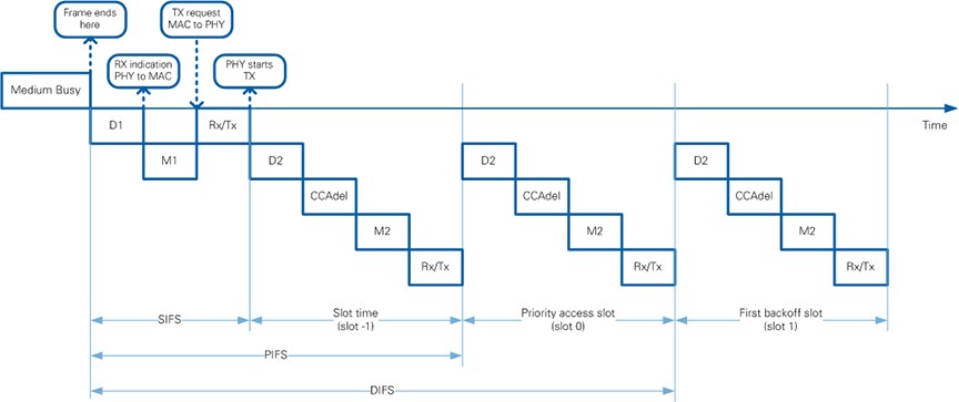
Transmission after frame reception refers, for instance, to receiving a data frame and transmitting an ACK frame with SIFS. Figure 10 shows such a scenario and the definitions of processing delays used in the IEEE 802.11 standard (refer to Figure 9-14 and Section 9.3.7 of [1]).
Figure 10: Timing relationships for transmission after frame reception
Table 2 summarizes the requirements of the standard and compares it to the values of the 802.11 Application Framework. The RX and TX PHY delays, aRxPLCPDelay and aTxPLCPDelay respectively, are comprised of processing delays of the I/Q Processing modules and Bit Processing Modules (refer to Sections 4.1.1 and 4.1.2 for more information). It is assumed that separate RF channels are used for RX and TX, and no RX/TX switch is used. Therefore, aRxTxSwitchTime and aTxRampOnTime are assumed to be zero. The assumption for D1 being equal to 12.0 µs is calculated from the relation SIFS = D1 + M1 + Rx/Tx.
| Name | Content | Assumption of IEEE 802.11 standard (Section 18.4.4 of [1]) | Value for 802.11 Appl. Framework |
| D1 | aRxRFDelay + aRxPLCPDelay IQ proc. + aRxPLCPDelay bit proc. | ~ 12.0 µs | 0.68 µs + 2.87 µs + 8.36 µs = 11.91 µs |
| M1 | aMACProcDelay 1 | < 2.0 µs | < 2.0 µs |
| Rx/Tx | aTxPLCPDelay bit proc. + aTxPLCPDelay IQ proc. + aRxTxSwitchTime + aTxRampOnTime + aTxRFDelay = aRxTxTurnaroundTime | < 2.0 µs | 0.0 µs + 0.0 µs + 0.0 µs + 0.0 µs + 1.29 µs = 1.29 µs |
| Sum | 16 µs | 15.2 µs* |
Table 2: Timing budget for transmission after frame reception
* MAC TX timing control ensures that interframe-spacing and slot timing requirements from IEEE specifications are met.
3.3.2.2 Timing Budget for Transmission after Channel Sensing
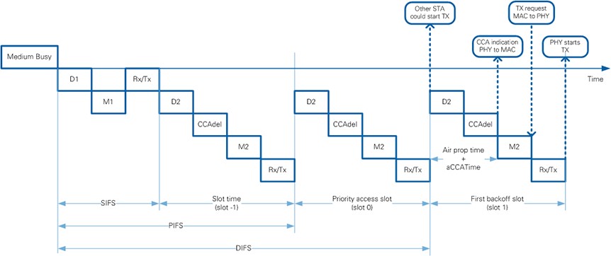
Transmission after channel sensing refers to situations such as transmitting a data frame after a backoff procedure. Figure 11 visualizes such a scenario and the definitions of processing delays used in the IEEE 802.11 standard (refer to [1] Figure 9-14 and Section 9.3.7).
Figure 11: Timing relationships for transmission after channel sensing
Table 3 summarizes the requirements of the standard and compares it to the values of the 802.11 Application Framework. These requirements assume that D2 + CCAdel = Air Propagation Time + aCCATime, which can be derived from the definitions given in Section 9.3.7 of [1]. aCCATime refers to the time needed for performing the CCA operation.
| Name | Content | Assumption of IEEE 802.11 standard ([1] Section 18.4.4) | Value for 802.11 Application Framework |
| Air Prop. Time | << 1.0 µs | Assume for instance 0.2 µs for 60 m distance | |
| aCCATime | CCA detection time | < 4.0 µs | < 2.0 µs |
| M2 | aMACProcDelay 2 | < 2.0 µs | < 2.0 µs |
| Rx/Tx | aTxPLCPDelay bit proc. + aTxPLCPDelay IQ proc. + aRxTxSwitchTime + aTxRampOnTime + aTxRFDelay = aRxTxTurnaroundTime | < 2.0 µs | 0.0 µs + 0.0 µs + 0.0 µs + 0.0 µs + 1.29 µs = 1.29 µs |
| Sum | 9 µs | 5.5 µs* |
Table 3: Timing budget for transmission after channel sensing
* MAC TX timing control ensures that interframe-spacing and slot-timing requirements from IEEE specifications are met.
3.3.3 Level Plan and Baseband Operating Points
3.3.3.1 DAC headroom, ADC headroom, signal power
The D/A converter (DAC) and A/D converter (ADC) should operate in a manner that avoids clipping and saturation of the outgoing and incoming signal, respectively. For proper adjustment of the DAC and ADC operating points, consider the following factors:
- OFDM has a high peak-to-average power ratio approximately between 9 dB to 12 dB. This range implies that a DAC headroom of 15 dB would avoid clipping.
- On the receiver side, signals on adjacent channels can occur that are 10 dB higher than the desired signal. Having an ADC headroom of 25 dB would also handle such signal constellations without running the ADC into saturation. For example, with an ADC resolution of 14 bits (as for the USRPs) and a noise figure of approximately 9 dB, approximately 8 effective bits available are in the baseband processing, which is sufficient for up to 256-QAM.
3.3.3.2 Reference signals according to IEEE 802.11a/ac
TX and RX IQ and bit processing and the related submodules of the 802.11 Application Framework follow the power normalization of the test vector generation tool provided by IEEE [3]. The test vector generation tool follows Equation (22-11) of Section 22.3.7.4 of [2] and, hence, the power of the complex-valued baseband signal is normalized to be equal to 1. TX and RX IQ and bit processing and the related submodules of the 802.11 Application Framework are tested against vectors generated by this tool. For any extension towards standard-compliant PHY features, NI strongly recommends that you test against vectors generated with this tool.
3.3.3.3 Complex Fixed Point (format, precision)
The mixed-signal processing output data type is a <1.15> fixed-point value. The peak-to-average power ratio of OFDM (refer to Section 3.3.3.1) means that the output must be extended by two bits in the integer part. Because each bit of a complex data type corresponds to 6 dB in signal power, this fact adds a headroom of 12 dB for the numeric representation. The data path interface between the baseband and mixed-signal processing consists of a <3.13> fixed-point value on both the TX and RX path. The conversion is done by reinterpretation of the 16 bits. The <3.13> fixed-point format allows you to compare against the reference signal of [3] (refer to Section 3.3.3.2). Furthermore, changing between simulation and operation mode does not require a change in scaling. In general, the precision of the fixed-point logic follows the fixed-point requirements of the implemented algorithms, and it is not optimized regarding to resource usage.
More information about fixed-point formats and related precisions to avoid clipping and saturation can be found in the following sections:
- Table 5 of Section 4.1.1.4 referring to synchronization,
- Table 6 of Section 4.1.1.5 referring to RX IQ processing
- Table 12 of Section 4.1.2.6 referring to TX IQ processing.
3.3.4 Channelization
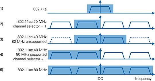
The different supported channelization options are illustrated in Figure 12.
For the 802.11ac format, the PHY RX must dynamically switch based on the channel bandwidth information in VHT-SIG-A. This switching is performed by selecting the correct range in the frequency domain without changing the RF front end center frequency, for example, switching between options 2, 4 and 5 in Figure 12. Therefore, you must set the RF front end frequency to an 802.11 channel, based on the widest supported bandwidth of the device. Use the channel sets given in the tables in Annex E of [2]. Otherwise, the wrong set of 20 MHz subbands could be concatenated for 40 MHz transmissions with other devices.
Figure 12: Channelization used in the Application Framework
The 256-point FFT of the PHY covers 80 MHz bandwidth. Based on the 20 MHz bandwidth of the 802.11a signal, the 80 MHz bandwidth can be divided into four subbands of 20 MHz (trapezoids in Figure 11). The parts highlighted in blue are actually used by the PHY, and the rest is filled with zeros. Two controls on the FPGA top level are used to choose one of the illustrated options. The switch control DC centered signal determines if the 802.11 channel center frequency equals the RF center frequency. The numeric control channel selector determines which subband is used as the primary subband. The resulting configuration for each option is listed in Table 4.
| Option | Bandwidth | 80 MHz realtime bandwidth supported | DC centered signal | Channel selector | Difference between RF center frequency and 802.11 channel center frequency |
| 1 | 20 MHz | N/A | Enabled | N/A | 0 MHz |
| 2 | 20 MHz | Yes N/A N/A Yes | Disabled | 0 1 2 3 | -30 MHz -10 MHz 10 MHz 30 MHz |
| 3 | 40 MHz | No | Disabled | N/A | 0 MHz |
| 4 | 40 MHz | Yes | Disabled | 0,1 2,3 | -20 MHz +20 MHz |
| 5 | 80 MHz | Yes | Disabled | N/A | 0 MHz |
Table 4: Configuration for channelization options
Option 1 is limited to the 802.11a format, and the DC-centered switch is enabled. The channel selector control is ignored for 802.11ac applications. The signal is centered within the frequency domain. Set the center frequency of the RF front end to the center frequency of the 802.11 channel as given in Annex E of [1].
All other options correspond to the 802.11ac format and require the DC centered switch to be disabled. The channel selector control selects the primary subband numbered from zero to three, which is used for non-HT reception.
For version 2.0 and 2.0.1, options 2 and 3 are valid for all RF devices. Set the RF front end center frequency to the center of a 40 MHz wide 802.11 channel. Subbands 1 and 2 are used for non-HT portion of the VHT format preamble transmission as described in Section 22.3.8.2 of [2]. VHT 20 MHz mode uses the primary subband only.
For USRP devices and FlexRIO devices capable of 80 MHz realtime bandwidth, you can select options 2, 4, and 5. The RF front end center frequency should be set to the center of an 80 MHz wide 802.11 channel. Subbands 0 to 3 are used for an 80 MHz wide non-HT VHT format preamble transmission as described in Section 22.3.8.2 of [2]. VHT 40 MHz mode uses subband 0 and 1, or 2 and 3, based on the channel selector. VHT 20 MHz uses the primary subband only.
Note that in the FPGA bitfiles included in the Application Framework project template, 80 MHz bandwidth support is disabled, so only options 1 to 3 are applicable. To enable options 4 and 5, the bitfile must be rebuilt with the 80 MHz Boolean enabled in the supported bandwidth cluster.
3.3.5 Global Timestamp
The system generates a global timestamp which is derived from the Data Clock (refer to Figure 8). Its granularity is 0.1 µs, and it is used as a time base of MAC modules and the event tracing.
4 Implementation Details
4.1 FPGA
4.1.1 RX
4.1.1.1 Overview
The RX baseband is operating in the baseband clock domain of 250 MHz. The RX baseband block diagram is shown in Figure 13. Blue arrows indicate the data path while yellow ones are connected to the control path. Details about the information are available in the following sections.
The data source block selects the source for the receiver. Data can be taken from RF, from the TX baseband using internal loopback, or from the host or by using a host to target FIFO. The stream always has a sample rate of 80 MS/s for all sources. The synchronization detects the packet start and compensates an estimated carrier frequency offset. In parallel, the power measurement block calculates the received signal power. The stream is given to the RX I/Q Processing block, where the samples are transferred to the frequency domain. Then channel estimation, equalization, and phase tracking is done. The constellation with field assignment information is provided to the RX Bit Processing block. Inside this block the modulation is reversed, the bits are deinterleaved, decoded using a Viterbi decoder and descrambled. This bit stream is given to the RX PHY state machine. This state machine interprets the signal fields, such as L-SIG, VHT-SIG-A, and so on, in the PPDU and generates control information for I/Q processing, bit processing, and MAC. The PSDU, which can be MPDU or A-MPDU, is removed from the bit stream and delivered to the MAC as unsigned bytes. The MAC interprets the header information of the PSDU and transfers data to the Host application using the LabVIEW target-to-host interface.
Every module is designed to keep up with the data rate from the upstream module, so there is no need for throttle control inside the modules. The timing of the transfers is described in the following sections.
Figure 13: RX Baseband block diagram
4.1.1.2 Power Measurement
The power measurement module calculates the baseband signal power and the RF input power. The block diagram is shown in Figure 14.
Figure 14: Power Measurement block diagram
Based on the incoming samples, x, the signal power, s, is calculated over a window of 64 samples as described in Equation 1. The output of this calculation is updated after 64 samples arrive. The next step is the iterative calculation of the logarithm to the base of 10. The value of s shifts n times to the left until the most significant bit (MSB) contains a one. The number of shifts, n, and a look-up table (LUT) of the six MSBs of the shifted value s are used to calculate the signal power p in logarithmic scale. This value represents the baseband signal power in dBFS.
Equation 1: Signal Power Calculation
Based on p, the RF input power r is calculated using the power calibration offset (configured from the host) and the RF gain (see Equation 2) provided by the AGC. Both values are given from the host. The analog gain value is subtracted from p because applying gain before ADC means that the RF input power is lower than the measured signal power. The power calibration offset is based on the calibration data of the device. It maps the baseband signal power at minimum gain to the corresponding reference power level4 at the RF input port. This mapping is assumed to be linear at all gain levels.
Equation 2: RF input power calculation
The value of r is compared against the given CCA energy threshold. If this threshold is exceeded, the CCA energy detect signal is asserted. Together with the baseband and the RF power, this value is available at the output of the Power Measurement VI.
4.1.1.3 AGC
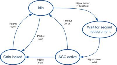
The AGC (Automatic Gain Control) is used to ensure that the operating point of the system keeps in an optimum range. Therefore, it is able to apply RX RF input gain values from 0 to 31.5 dB. The module is implemented as a simple state machine as shown in Figure 15 .
Figure 15: AGC state machine
In the Idle state, the maximum possible gain value (31.5 dB) could be applied to make sure that very low powered incoming packets will not be missed. When the measured input power exceeds a threshold level that can be configured from the host, the AGC waits for a second power measurement. This second value will be used to determine the applied gain for the current packet based on a host configurable mapping table. In the current implementation the AGC is able to apply 4 different gain levels: 0 dB, 10.5 dB, 21 dB or the maximum value of 31.5 dB.
If the gain value is changed within a valid frame, the frame would be corrupted. To mitigate that, the applied gain will be locked after receiving a packet start signal from the synchronization module. This lock will be released after the end of the frame is detected which is signalized by the same signal that also rearms the synchronization module.
4.1.1.4 Synchronization
The purpose of the synchronization module is to find the packet start in the continuous sample stream. The ideal position of the packet start for the implemented algorithm is in the center of the L-LTF field. It is the first sample of L-LTF-2 (second OFDM symbol of L-LTF).
The block diagram of the synchronization unit is shown in Figure 16 and details of data types, control information, and identifiers used in equations can be found in Table 5.
The synchronization is fed from the data source with a sample rate of 80 MS/s. In the baseband clock domain of 250 MHz, approximately every third sample is valid. Each VI must use the enable chain to update only on valid samples. The data rate is not changed by any VI.
Figure 16: Synchronization block diagram
| Module | Identifier | Output Data Type | Output Control Information |
| Autocorrelation | a | UFXP 2.14 | - |
| Timing Metric Calculation | tm | FXP 2.6 | - |
| Timing Metric Peak Search | - | U16 FXP 2.20 | Peak index CFO |
| Timing Metric Valley Search | - | U16 | Valley index |
| Timing Metric Evaluation | - | Boolean U16 FXP 2.20 | CCA signal detect Packet start sample index CFO |
| CFO Removal | - | CFX 3.13 | - |
| Frame Alignment | - | CFX 3.13 | Packet start |
Table 5: Synchronization Data Types and Control Information
The synchronization block is implemented in two parallel paths (refer to Figure 16) to minimize the latency on the data path. The upper path finds the packet start sample index and estimates the carrier frequency offset (CFO) based on the Schmidl and Cox algorithm [4]. These estimates are used by the lower path, which is the main data path, to compensate CFO and generate the packet start pulse for downstream modules.
For testing purposes, there is a bypass for the synchronization block where the packet start index can be given from the host. This path is not included in Figure 15. Use this bypass in combination with RX samples from the host or internal loopback to characterize the RX baseband without the impact of synchronization algorithms.
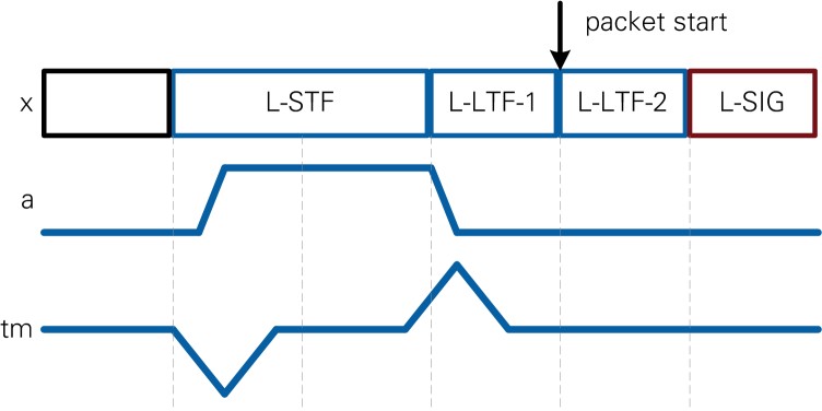
As shown in Figure 16, the upper path of the synchronization block starts to calculate the autocorrelation of the received signal x (see Equation 3). As the length of one period of the non-HT short training field is 64 samples at 80 MS/s sample rate (refer to Section 18.3.3 in [1]), the length of autocorrelation window CP (see Equation 3) is set to 64. The normalized magnitude and the phase of the autocorrelation window, s, are given at the output of the autocorrelation module for each sample. Under ideal conditions, this autocorrelation scheme results in a normalized magnitude equal to 1 as shown in Figure 17.
Equation 3: Synchronization Autocorrelation
Figure 17: Simplified signal charts of synchronization
To find the transition from L-STF to L-LTF, a so-called synchronization timing metric is calculated based on the magnitude of the normalized autocorrelation, as shown in Equation 4. The ideal behavior of this timing metric, tm, is also shown in Figure 16.
Equation 4: Synchronization Timing Metric
Based on the indices of the minimum and maximum value of this metric and the distance between minimum and maximum, the sample index of the packet start is calculated using the following steps:
- The timing metric peak search looks for the valley of the timing metric. This valley is 2 x CP samples after the start of LSTF. A valley is found if a given number of samples is under a defined threshold. The sample index of the center of all samples being under the threshold is given by the valley search as valley index. A 16-bit wide wrapping counter is used to give that index. The phase of the timing metric is captured on the first value that exceeds the threshold.
- A peak search is also used for the timing metric. Under ideal conditions, this index is CP samples after the start of LLTF. It uses the same principle as the valley search.
- Those two search results are combined in the Timing Metric evaluation. This module checks the distance between valley and peak which has to be within a given range of 9 x CP ± CP. As an additional check, the autocorrelation value must be under a given threshold. This check is valid for a packet start because during L-LTF the autocorrelation reports a low value.
Based on this algorithm and corresponding processing delays, the packet start sample index is calculated and given to the Frame Alignment module. During the calculation, the number of samples to cut into the OFDM guard interval is taken into account.
In addition to timing estimation, the phase of the autocorrelation is averaged over CP values and used for CFO estimation. This CFO estimation is based on the phase output of the peak search.
In the lower path of the synchronization block, the estimated CFO is compensated by applying a digital frequency shift. The CFO estimate is used for all OFDM symbols of the entire packet. The Frame Alignment module generates the packet start trigger pulse at the sample index given by the timing metric evaluation.
After the synchronization has indicated a packet start signal, further triggering of packet start signals is blocked until the synchronization is rearmed by the PHY RX end indication, generated at the end of the packet. This blocked status is indicated by the asserted CCA signal detect signal.
Figure 18: Synchronization latency
Synchronization Latency
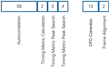
The latencies for the different modules in the Synchronization block are illustrated in Figure 18. The left part of the figure contains the modules of the upper path. The latency of those modules totals 68 clock cycles. Given the sample rate of 80 MS/s at 250 MHz clock rate, this time is equivalent to about 22 samples. Since the peak of the timing metric is located 256 samples before L-LTF-2, the packet start index is calculated before the packet start signal is asserted, and there is no effective delay.
The latency of the lower data path is shown in the right part of Figure 18. This latency increases the length of the RX processing path by 15 clock cycles.
4.1.1.5 RX IQ Processing
The receiver RX IQ Processing block purpose is to restore the transmitted I/Q constellation. The block diagram is shown in Figure 19. Details of data types, control information, and identifiers used in equations are presented in Table 6.
Figure 19: RX IQ processing block diagram
| Module | Identifier | Output Data Type | Output control information |
| Synchronization | - | CFX 3.13 | Packet Start |
| Sample Timing Generation | - | Sample Timing | |
| Cyclic Prefix Removal | - | ||
| FFT | R | CFX 4.21 | OFDM symbol index |
| Demapper | - | Field Map Subcarrier Timing | |
| Channel Estimation | Hest | Subcarrier index | |
| Channel Equalization | Yest | CFX 2.14 | Field Map Subcarrier Timing |
| Pilot Phase Estimation | ß | FXP 1.14 | - |
| Phase Correction | Xest | CFX 2.14 | Field Map Subcarrier Timing |
| VHT-SIG-A2 Rotation | - |
Table 6: RX IQ Processing Data Types and Control Information
The Sample Timing Generation module gets samples from the Synchronization module along with the packet start index. It starts passing samples to downstream modules as soon as the packet start signal is asserted. It stops passing samples as soon as the last OFDM symbol is finished whose index is given by the RX PHY state machine. The control information is carried by the sample timing cluster, which contains the following elements:
- OFDM symbol index
- Sample index (within the OFDM symbol; 0 to 319)
- Packet start flag
- OFDM symbol start flag
- Valid flag
The sample index is used by the Cyclic Prefix Removal module to invalidate the first 64 samples of each OFDM symbol.
The next downstream module is the FFT, which is a wrapper for the Xilinx FFT core. It contains a 256-point FFT operation using a Radix 4, Burst I/O architecture. A toggling negation realizes the FFT shift to have the DC at the 128th output value. The FFT starts execution as soon as 256 samples are provided. During the execution, no samples are taken on the input. A FIFO is placed before the input to capture the samples that arrive in the meantime. On finishing execution, the 256 subcarriers are provided at the output consecutively. The OFDM symbol index from the incoming sample timing cluster is passed through this module, parallel to the data stream. The maximum gain of the FFT is 256 if the energy is limited to only one subcarrier. Therefore, the fixed point data type is extended by nine bits to capture this output dynamic range of the FFT module. The output of the FFT is divided by 256 to have the same scaling as on the input of the IFFT in the transmitter chain. The resulting fixed point format is <4.21>.
The Demapper block aligns two control information clusters with the data stream. The first cluster is the subcarrier timing cluster, which contains the following elements:
- OFDM symbol index
- Subcarrier index (0 to 255)
- Frequency offset index (named k in equation 18-23 of [1] and [2]; -128 to 128)
- OFDM symbol start flag
- Valid flag
The frequency offset index is generated based on the control information from the RX PHY state machine. The second control information cluster is the field map. This cluster is made up of Booleans, and each Boolean represents one field of the 802.11 packet structure, such as L-SIG, L-LTF, VHT-SIG-A, pilot subcarrier, or data subcarrier. Similar to a one-hot code, only one of these Booleans is asserted for each sample. The packet structure is known to the Demapper module. Downstream modules can take this field map to filter for specific fields, such as the pilot subcarriers.
The channel estimation is computed using the second L-LTF OFDM symbol for 802.11a and VHT-LTF for 802.11ac. The inverse channel transfer function is calculated for each subcarrier R individually using the L-LTF definitions L from Section 22.3.8.2.3 of [2] as shown in Equation 5. The signal names are included in Figure 18. The frequency offset index k from the subcarrier timing is used. The channel estimation block is implemented in a parallel path to minimize latency to the data path. The values of Hest are given to the channel equalization module where they are stored in memory. They have the same data type as the incoming subcarriers. Beginning with the L-SIG, the channel equalization uses those values to apply zero forcing to get signal Yest. The fixed point format of <2.14> is sufficient to represent the values of Yest. Larger values are saturated.
Equation 5: Channel Estimation and compensation
The signal Yest is passed to the pilot phase modules that follow the same structure as the channel estimation and equalization. Removing the cyclic prefix leads to a phase jump between consecutive OFDM symbols due to the residual carrier frequency offset after the synchronization. The phase for the current OFDM symbol an is calculated based on the pilot sequences P. These sequences are taken from Section 18.3.5.10 of [1] and Section 22.3.10.10 of [2] at the frequency offset index k. The phase offset between OFDM symbols is compensated by adding the difference to the last phase estimation from OFDM symbol n - 1. The estimated phase ß of OFDM symbol n is applied to the OFDM symbol n + 1 by the Phase Correction module. This operation does not change the magnitude of the values, so the fixed point format is kept.
Equation 6: Phase estimation and compensation
As the last step of the RX I/Q processing, the clockwise rotation of VHT-SIG-A2 (refer to Section 22.3.4.5 of [2]) is reversed.
| Module | Output timing |
| Sample Timing Generation | ~ 1 sample / 3 clock cycles (320 samples per OFDM symbol) |
| Cyclic Prefix Removal | ~ 1 sample / 3 clock cycles (256 samples per OFDM symbol) |
| FFT | 256 subcarriers / OFDM symbol burstwise |
| Demapper | |
| Channel Estimation | |
| Channel Equalization | |
| Pilot Phase Estimation | 1 phase estimate / OFDM symbol |
| Phase Correction | 256 subcarriers / OFDM symbol burstwise |
| VHT-SIG-A2 Rotation |
Table 7: RX IQ Processing Transfer Timing
The timing of the data stream is changed inside the RX I/Q Processing module. A summary for all submodules is given in Table 7. The input is given by the digital downconversion at a sample rate of 80 MS/s. The Cyclic Prefix Removal module removes 64 samples from the stream. Because of the chosen FFT architecture configuration the output of the Xilinx core is given burstwise. This transfer timing is kept for all downstream modules. The only exception is the Pilot Phase Estimation module that computes one phase estimate per OFDM symbol.
RX I/Q Processing Latency
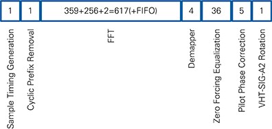
The overall latency of the RX I/Q Processing module for the last sample of the OFDM symbol is 665 clock cycles as shown in Figure 20. The FFT latency is smaller than reported by the Xilinx IP Generator, and this latency includes loading of all 256 samples. During the packet, the FFT executes and unloads samples in 617 clock cycles after the last sample arrived. The remaining clock cycles per OFDM symbol are used to transfer data from the input FIFO to the FFT core. By the time the last sample is available on the input, the FIFO is empty, and it is passed to the core as fast as possible. The delay of the FIFO is unknown, which is indicated in Figure 20. All other modules have a fixed latency.
Figure 20: RX IQ Processing Latency
4.1.1.6 RX Bit Processing
The RX bit-processing chain deinterleaves, decodes, and descrambles the data. It provides the received bits to the RX PHY state machine and the PSDU bytes to the MAC. The block diagram is shown in Figure 21. Details about data types and control information is given in Table 8.
Figure 21: RX Bit Processing block diagram
| Module | Output Data Type | Output control information |
| RX IQ Processing | CFX 2.14 | Field Map Subcarrier Timing |
| Packet Termination | ||
| Align Configuration | Bit Processing Configuration | |
| LLR Demapper | FXP8.0 Array (8 elements) | |
| Softbit Serializer | FXP8.0 | |
| Deinterleaver | ||
| Depuncturing | FXP8.0, Boolean Array (2 elements) | |
| Viterbi | Boolean | |
| Descrambler | ||
| PSDU Masking | U8 | - |
Table 8: RX Bit Processing Data Types and Control Information
The first module of the chain is the Packet Termination module. It passes all samples that have OFDM symbol indices in the subcarrier timing cluster below the value given from the RX PHY state machine. Passing only these samples ensures that the packet end is correctly processed. If you abort the current packet reception, this module terminates all I/Q data by setting the last OFDM symbol index to 0.
The next block is the Align Configuration module. It has two functions. First function is to align the bit-processing configuration cluster from the RX PHY state machine with the start of a new OFDM symbol. All other control information is terminated in this module. The bit-processing configuration is transferred parallel to the data stream, and it contains the following information:
- Packet format
- Bandwidth
- Modulation
- Coding rate
- PSDU length (in bytes)
- Valid bits in current OFDM symbol
- Descrambler enable flag
- Viterbi flush required flag
The second function is the filtering of all noncoded fields for downstream modules. It uses the field map provided by the RX I/Q processing chain.
The I/Q samples in the coded fields are processed by the log-likelihood ratio (LLR) Demapper block. Based on the given modulation scheme, an array of up to eight softbits is given at the output. The data type of each softbit is unsigned 8-bit integer.
The Softbit Serializer module takes this array of softbits and provides the serialized stream on the output. The number of valid softbits in the array is derived from the modulation. An internal FIFO is used to buffer softbits on the input.
The Deinterleaver module reverts the BCC interleaver operations defined in Section 18.3.5.7 of [1] and Section 22.3.10.8 of [2]. The write operation into the memory is based on equation 22-82 of [2], which reverses the second permutation. The read operation is based on equation 22-77 of [2], which reverses the first permutation. Reading is started as soon as all softbits of the current OFDM symbol are saved to memory. A double page memory is used, which enables reading and writing at the same time.
Based on Figure 18-9 and 20-11 of [1], the Depuncturer module converts the incoming bit stolen data sequence to the bit inserted data sequence. Each bit gets a puncturing flag attached depending on whether it was transmitted or left out. One element of A and the corresponding element of B are combined into an array of two elements, where A and B are as defined in Figure 18-9 and 20-11 of [1].
The array is given to the Viterbi wrapper, which converts the softbits into the required format and inserts a softbit value of Zero (the maximum uncertainty value) for all punctured bits before feeding the sequence to the Viterbi decoder (see 7.3 for implementation details). After the last softbit of the current code word, the Viterbi is flushed to get the remaining bits out of the core. For flushing, strong zeros are pushed to the input with data bit flag set to FALSE. The data bit flag has the same latency as the data path. Hence on the output of the core, the data bit information can be used to filter out the zeros from the flushing operation. The bits of the code word are provided at the output.
The Descrambler module processes the bits at the output of the decoder. If the scrambler is disabled, the input bits are bypassed to the output. On activation, detected by the rising edge of the enable signal, the Descrambler module assumes it is receiving a packet starting with the SERVICE field and uses the first seven bits to extract the scrambler seed. Those initial bits are overwritten by zeros. Afterward, all bits are descrambled with the recovered seed until deactivation.
The output is transmitted to the RX PHY state machine. Before sending to the MAC, the bit stream is filtered by the PSDU Masking module. The SERVICE, TAIL, and PAD fields are removed, and the bits are concatenated to bytes. The length of the PSDU is given by the configuration. Padding bits are removed. For the 802.11ac format, parts of the PAD field may be included in the PSDU data stream (refer to Section 4.1.1.7 for more information).
| Module | Output Timing |
| Packet Termination | 256 subcarriers burstwise / OFDM symbol |
| Align Configuration | NSD data subcarriers / OFDM symbol (48-108) |
| LLR Demapper | |
| Softbit Serializer | NCBPS coded softbits / OFDM symbol (48-864) burstwise; gaps due to pilots |
| Deinterleaver | NCBPS coded softbits / OFDM symbol (48-864) burstwise |
| Depuncturing | NDBPS encoded stream values or data bits / OFDM symbol (24-720) Peak rate: 1 value / clock cycle |
| Viterbi | |
| Descrambler | |
| PSDU Masking | NDBPS/8 data bytes / OFDM symbol (3-90) Peak rate: 1 byte / 10 clock cycles |
Table 9: RX Bit Processing Transfer Timing
The output timing of the submodules is given in Table 9. The number of values depends on the format, bandwidth, and MCS. The referred variables can be found in Table 18-4, 18-5 of [1] and Table 22-30, 22-38 of [2]. In brackets, the minimum and maximum values are given indicating the valid range. The minimum value is based on L-SIG, which uses non-HT mode with MCS 0. The maximum value is based on VHT 40 MHz transmissions using MCS 9.
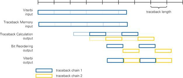
The RX I/Q Processing module provides 256 subcarriers in one burst. The first module that changes this pattern is the Configuration Alignment. Only subcarriers belonging to coded fields remain on the output. Since there are multiple pilot tones, this stream contains gaps. The serialized stream on the output of the Softbit Serializer module can have much more valid items per OFDM symbol. Nevertheless, the pilot gaps remain if you are using BPSK modulation, where each subcarrier is translated to one softbit by the LLR Demapper. The gaps are gone after the Deinterleaver module because the softbit stream is read burstwise from the internal memory. The Depuncturer adds gaps to this data stream when there are two valid bits of stream A and B available. Adding punctured bits does not produce gaps. The Viterbi generates data on the output as soon as traceback length input bits are provided to the intput. As a result, the output is given burstwise where each burst has traceback length bits. The concatenation to byte data type of the PSDU reduces the data rate by factor 8. At a coding rate of 5/6, the peak rate is reached.
Figure 22: RX Bit Processing Latency
Rx Bit Processing Latency
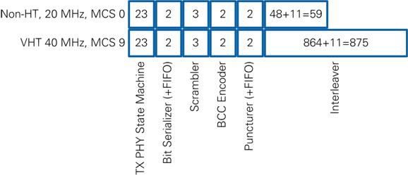
The latency of the RX Bit Processing chain depends on the format, bandwidth, and MCS. Similar to Table 9, Figure 21 refers to the two corner cases L-SIG and highest MCS at highest bandwidth. The latency is given for the last subcarrier of the packet generated by the RX I/Q Processing module. Most of the modules have a fixed latency.
The delay of the Softbit Serializer depends on the modulation. For BPSK, each subcarrier is mapped to one softbit so the serialization does not add any delay. The internal FIFO is empty when the last value arrives. The FIFO delay is unknown. The latency is 2 because of internal registers. For 256-QAM, each softbit array has to be split into eight softbits on the output. When the last value arrives, 108 (NSD) of 864 (NCBPS) softbits are processed on the output. The delay for the last softbit added with the two register stages results in 758 clocks latency.
The Deinterleaver has to store one complete OFDM symbol of softbits. The read operation starts as soon as the last value arrives. NCBPS softbits have to be read before the last sample is available on the output of the Deinterleaver. An additional latency of 11 is incurred because of the pipeline stages.
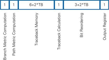
The latency of the Viterbi decoder is determined by the chosen traceback length. An additional latency of 15 is incurred due to pipeline stages (see 7.3 for implementation details).
The latency for other configurations can be calculated using Equation 7 with values from Table 18-4, 18-5 of [1] or Table 22-30, 22-38 of [2].
Equation 7: RX Bit Processing Latency
4.1.1.7 RX PHY state machine
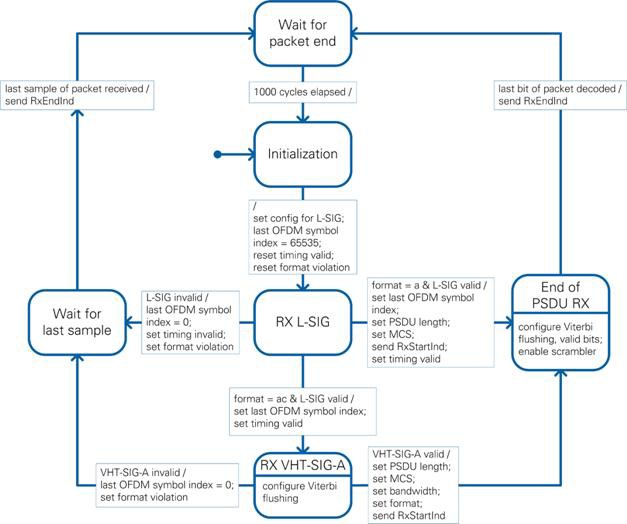
The RX PHY state machine, which is based on Figure 22-37 of [2], provides the configuration for RX IQ and RX Bit Processing modules and generates indications for the MAC. Notice that the synchronization is controlled indirectly by the state machine. The RX end indication is used to rearm the synchronization. Notice also that the PHY is not capable of decoding VHT MU PPDUs, so the reception of VHT-SIG-B is skipped as described in Section 22.3.21 of [2]. The state diagram is given in Figure 23. The word timing in this diagram refers to the timestamp when the last sample of the packet was received, which is included in the PHY RX end indication.
Figure 23: RX PHY state machine states
Initialization
This is the startup state. In this state, the internal configuration is reset such that it can receive the first coded field in the packet (L-SIG in the primary subband). This setting consists of the 802.11a format, 20 MHz bandwidth, disabled scrambler, and MCS 0. The unknown length of the packet means that the last OFDM symbol index is set to the maximum unsigned 16-bit integer value of 65,535.
RX L-SIG
As soon as the synchronization detects a packet, the processing chain uses the configuration from the Initialization state to provide the 24 bits of the SIGNAL field to the RX PHY state machine. The received bits are verified to be a valid L-SIG field based on Section 18.3.4 of [1]. The L-SIG check includes verifying the following conditions:
- R4 of the RATE field is one
- Bit 4 is zero
- SIGNAL TAIL field is all zeros
- Parity bit is matching
- LENGTH > 0
The result of the check is used as condition L-SIG valid in the state machine. As soon as this condition is evaluated the state machine leaves this state.
If L-SIG is invalid, the reception of the current packet is aborted. The last OFDM symbol index is set to 0. This forces the Sample Timing Generation module of the RX I/Q processing chain and the Packet Termination module of the RX bit processing chain to finish the current OFDM symbol and stop. Because there is no packet length information available at this point in time, the timing information is marked as invalid. Furthermore, the internal format violation flag is set.
If a valid L-SIG is received, the next state depends on the packet format selected from the host. In the 802.11a format, all necessary information is available from L-SIG interpretation to start reception of the data. The index of the last OFDM symbol is calculated based on equation 18-11 of [1]. This index as well as MCS and PSDU length are provided to the processing chain. In addition, the PHY RX start indication is generated, and the packet frame timing is set to valid.
If the L-SIG is valid and the format is set to 802.11ac, further information from VHT-SIG-A is needed to decode the packet. Only the index of the last OFDM symbol can be calculated, which also results in a known packet timing. The format still remains 802.11a because the VHT-SIG-A is coded like a L-SIG with MCS 0.
RX VHT-SIG-A
Similar to the RX L-SIG state, the processing chain is configured to provide the bits of the VHT-SIG-A to the RX PHY state machine. The code word of VHT-SIG-A is provided in two OFDM symbols. The Viterbi decoder flush required flag in the bit processing configuration cluster is set for the second OFDM symbol. This bit-processing configuration cluster is aligned with the data stream in the RX Bit Processing block by the Configuration Align Configuration module (see Section 4.1.1.6). Hence, accurate indication of the current OFDM symbol index is available from the RX Bit Processing module and can be used to set the Viterbi decoder flush required flag.
The 48 bits of the VHT-SIG-A are captured, and its validity is verified based on Section 22.3.8.3.3 of [2]. The condition VHT-SIG-A valid is based on the following checks:
- Bandwidth is supported by PHY
- Group ID indicates VHT SU PPDU (0 or 63)
- Short GI is set to zero (disabled)
- B2 is set to zero (BCC encoding)
- CRC checksum is matching
If VHT-SIG-A is invalid, the reception is aborted, similar to an abortion out of the L-SIG state, except the timing information is known from a successful L-SIG reception.
If VHT-SIG-A is valid, you can configure the bandwidth, format, MCS and PSDU length in the processing chain. Since there is no specific length information given in VHT-SIG-A, the PSDU length is calculated using Equation 22-112 of [2]. This PSDU length is greater or equal to the exact payload size. Padding bits are included in the PSDU and given to the MAC.
Wait for last sample
This state can abort a running reception when an invalid signal field occurs. The state machine waits until the Sample Timing Generation module of the RX I/Q Processing module indicates that the last sample of the current OFDM symbol has been processed. The global timestamp is captured at this point in time to provide the end of the packet as the new frame timing. The PHY RX end indication is generated using the internal information about format violation and timing validity in addition to this new frame timing.
End of PSDU RX
This field is entered when the signaling information was correctly received and the data field is to be decoded. Similar to the RX VHT-SIG-A state, flushing the Viterbi decoder is enabled only for the last OFDM symbol of the packet, which is identified by the last OFDM symbol index computed in RX L-SIG state. Furthermore, in 802.11a format, the number of valid data bits in the last OFDM symbol before tail and padding is known and configured to the Viterbi module so that the TAIL bits are the last to be decoded. For 802.11ac format, the padding is inserted before tail bits. The valid bits limitation is not used in this case. All bits of the last OFDM symbol are processed by the Viterbi decoder.
The state is left as soon as the PSDU Masking module in RX bit processing indicates that the last byte of PSDU has been decoded. A PHY RX end indication with the frame timing information is generated. Similar to the wait for last sample state, the frame timing is based on the global timestamp captured when the last sample of the packet was processed in Sample Timing Generation module in RX I/Q Processing.
Wait for packet end
The state is left after 1,000 clock cycles, which is the duration of one OFDM symbol. This waiting period is required because either the RX IQ processing or RX bit processing chain or both could still be working on samples that must be terminated before setting the configuration for a new L-SIG reception. Since the processing is based on OFDM symbol boundaries, after the duration of one symbol, all modules are in idle state.
4.1.1.8 Timing
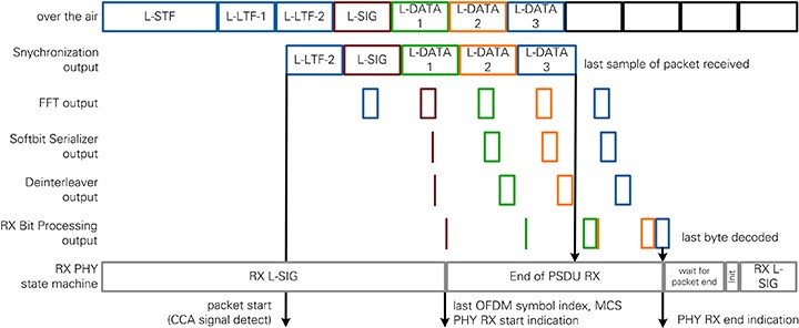
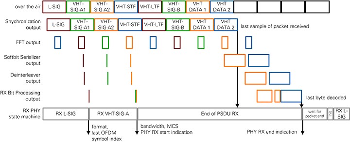
The overall timing of the RX chain including Synchronization, I/Q and bit processing, and the RX PHY state machine is shown in Figure 24 for 802.11a packets. Time is represented on the horizontal axis. On the vertical axis, several selected modules with important outputs or that change the transfer timing are displayed. The colored rectangles correspond to the data values of one OFDM symbol. The size and the placement among the time axis are related to the latencies and transfer timings of the modules. The black arrows show important control signals between processing chain and state machine and between PHY and MAC. The arrows are based on the timing information. Neither the start nor the end position has to be related to the module that generates or consumes this control information.
Figure 24: RX PHY Timing for 802.11a packets
Figure 23 shows the timing of the receiver for the packet of 802.11a with MCS 7 and NSYM=3. RF and Synchronization add the latency between over-the-air transmission and the synchronization output. The first OFDM symbol after the packet start is L-LTF-2. The RX PHY state machine has configured the RX IQ and Bit Processing modules to receive L-SIG.
As soon as the last sample of the L-SIG field is available in the FFT the execution starts. The burstwise unloading of data is done in parallel to reception of the next OFDM symbol on the FFT module input. L-LTF-2 is terminated in the Align Configuration module of the RX Bit Processing block.
As the first dynamic field, the L-SIG is the first field handled by the RX Bit Processing. L-SIG uses MCS 0, so it has only 24 data bits, and the latency is much smaller than one OFDM symbol duration. The decoding and flushing of the Viterbi decoder take most of the time. The RX PHY state machine can update the configuration cluster for the reception of the coded data symbols based on the L-SIG field contents long before the next OFDM symbol is unloaded by the FFT.
Starting with L-DATA-1, the RX Bit Processing chain uses MCS 7. This results in larger amount of bits on the Softbit Serializer module output. The Viterbi divides the bits into chunks of the traceback length. Because of this processing pattern, the output of the RX Bit Processing chain is not given OFDM symbol wise.
The code word ends in the last OFDM symbol, and the Viterbi is flushed. Due to padding bits, the decoding can end before the last bit has been received. The PSDU Masking module notifies the RX PHY state machine to send out RX PHY end indication with the timestamp of the last sample of packet and goes to wait for packet end state. The RX PHY state machine remains in this state to terminate the remaining bits of the last OFDM symbol out of the RX Bit Processing chain. After the Initialization state, the RX chain is ready to process a new packet.
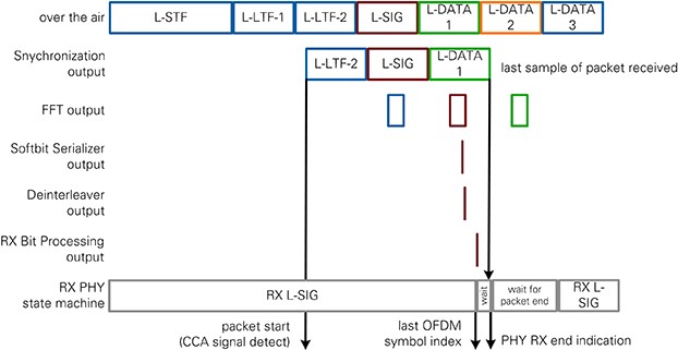
Figure 25: RX PHY Timing for invalid packets
Figure 24 illustrates the termination of the reception in case L-SIG was not valid. An invalid VHT-SIG-A is handled similarly. Like in Figure 24, L-SIG is provided to the RX PHY state machine. Once it is determined that L-SIG field contents are invalid, the last OFDM symbol index is set to zero, and the state machine goes to wait for last sample state.
At this point in time, the FFT may be filled with data from the next OFDM symbol and cannot be aborted immediately. The Sample Timing generation module in RX IQ Processing block completes the current OFDM symbol and notifies RX PHY state machine after the last sample. RX PHY state machine switches to wait for packet end state and waits for the duration of one OFDM symbol. During this time the FFT unloads the remaining data. This data is terminated in the Packet Termination module of the RX Bit Processing chain.
Figure 26: RX PHY Timing for 802.11ac packets
The reception of an 802.11ac packet with a bandwidth of 40 MHz at MCS 9 is shown in Figure 25. Since the process before L-SIG is equal to Figure 24, it is left out. After the L-SIG field, the RX PHY state machine switches to RX VHT-SIG-A state and updates the format to 802.11ac. The Demapper module in the RX I/Q Processing chain enumerates further subcarriers for 802.11ac. The timing of VHT-SIG-A reception is similar to L-SIG in RX IQ and Bit Processing chain. Because the VHT-SIG field only has a small number of bits and the Viterbi code is flushed at the end of VHT-SIG-A2, the 48 bits arrive in one bust at the RX PHY state machine.
If VHT-SIG-A is determined to be invalid, the reception would be aborted similar to the L-SIG invalid case illustrated in Figure 24. In this case, VHT-STF would be the last OFDM symbol getting out of the FFT.
If VHT-SIG-A is valid, the parameters bandwidth and MCS are obtained from the field and used to set the configuration clusters for the processing chain. PHY RX start indication is sent to MAC and the RX PHY state machine transitions to the End of PSDU RX state and waits for end of decoding.
The next OFDM symbols contain training sequences and VHT-SIG-B. This information is not handled in RX Bit processing chain.
In this example, the RX Bit Processing is for MCS 9, which consists of 256-QAM modulation. This scenario results in a large number of bits generated by the LLR Demapper, which are serialized by the Softbit Serializer. Reading and writing the Deinterleaver memory overlaps for this large number of bits is the reason for having a double page memory in this module. The Viterbi is flushed on the last OFDM symbol as in 802.11a format. RX PHY end indication is sent by the state machine if the last byte has been provided to MAC.
4.1.1.9 MAC RX
The module MAC RX implements low-level latency-critical MAC reception functionality, i.e. validation and recognition of received packets and triggering of ACK responses. Input to the module are SDUs delivered from the PHY together with associated control information. The MAC RX module performs frame validation, consisting of subframe detection for packets received in 802.11ac format and the FCS check for all received MPDUs. Subsequently MPDU type recognition is performed. For supported frame types, MAC header evaluation and address filtering is done. Finally, MSDU extraction is performed by a configurable filter operation. In addition to these packet-handling related functionalities, the module MAC RX also handles CCA information from the PHY RX and forwards frame timing information from the PHY RX to the MAC TX.
As shown in Figure 27, the module MAC RX consists of five major submodules:
- A-MPDU Frame Validate
- MPDU Validate
- MPDU Recognize
- MPDU Filter
- Channel State
All five submodules are described in more detail in the following sections. Notice that the overall internal structure of MAC RX roughly follows the concept of the IEEE 802.11 SDL specifications. Refer to Section J.5 of [1] for more information about the SDL specifications.
Figure 27: MAC RX block diagram
The module A-MPDU Frame Validate is only applicable for packets received in 802.11ac format. It checks the MPDU delimiter and provides the contained information to subsequent modules. For received packets in 802.11a format, the module passes all data through without any change. For the 802.11 Application Framework version 2.0 and 2.0.1, this module can handle only A- MPDUs with one A-MPDU subframe, as in one MPDU.
The module MPDU Validate performs frame validation by means of the FCS field. The FCS check is done based on IEEE 32-bit CRC as specified in [1] Section 8.2.4.8. During the check, the 4 FCS bytes are removed. The module implements a small state machine to extract control information, such as the frame end timing validity and value, from the MPDU start indication primitive and the PHY RX end indication primitive. This information is collected in the RX info indication and forwarded to the Channel State module.
The module MPDU Recognize detects the frame type of received MAC PDUs. For supported frame types, MAC header evaluation is executed, including destination MAC address check (for all frames) or Source MAC address extraction (for frames with address field 2, such as data frames). Currently supported frame types are Data and ACK. For Data frames received with correct FCS and a matching address, an ACK transmission request is generated and forwarded to MAC TX.
The module MPDU Filter implements a configurable filter operation on received MPDUs. The filter can be configured to block MPDUs with FCS error, address mismatch or unsupported frame type. The filter also allows removal of MAC headers. The filtered received data and control information is converted into a serial data stream for transferring it using a target-to-host FIFO to the host.
The default filter configuration for the 802.11 Application Framework is as follows:
- Remove header: TRUE
- Block unsupported frame types: TRUE
- Block FCS errors: TRUE
- Block address mismatch: TRUE
- Block header recognize error: TRUE
As a result of this configuration, only the frame body of received Data MPDUs with correct FCS and matching address is sent to the host. For the 802.11 Application Framework version 2.0 and 2.0.1, this is sufficient since no further MAC operation is implemented on the host. If you want to perform MAC operations on the host, the filter configuration has to be adapted. If for example the MAC header field Duration is evaluated on the host, remove header must be set to FALSE. Then the MAC header of ACK and Data frames are forwarded to the host. After evaluating the Duration field, the host completes MAC header removal for Data frames.
The module Channel State gathers CCA status information, including energy detection and signal detection, and information about received frames, including frame end timing validity/value, and DIFS/EIFS indicator, and then it provides it to MAC TX.
4.1.2 TX
4.1.2.1 Overview
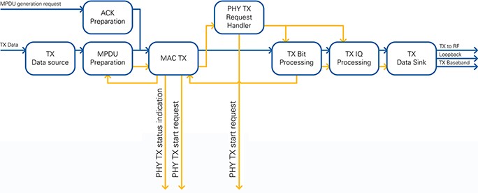
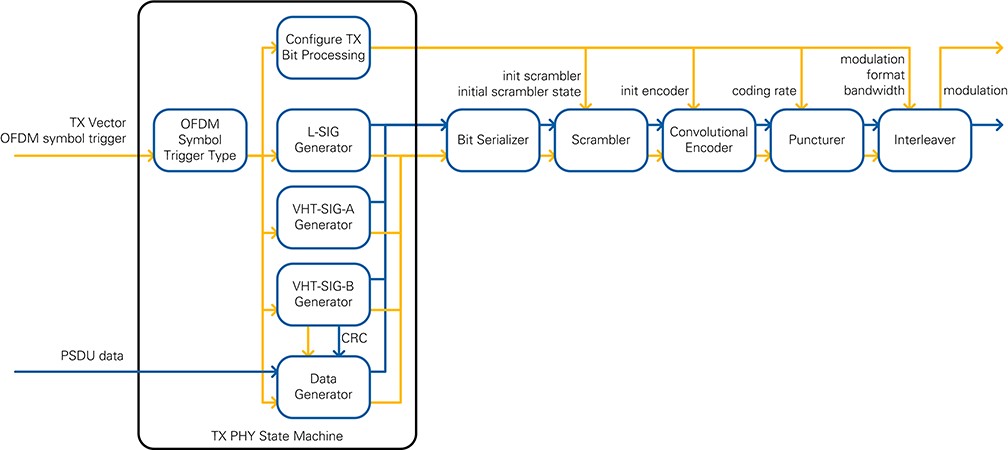
The TX baseband operates in the baseband clock domain of 250 MHz. Its block diagram is shown in Figure 28.
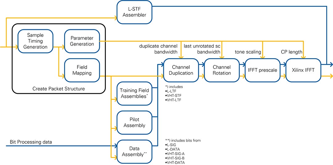
The data source block selects the source for the transmitter. Data is always taken from a host to target FIFO, or you can disable this feature when the MAC TX is bypassed. The MAC TX accepts TX requests to start after SIFS (ACK frames) or after backoff procedure (data frames). It multiplexes the requests in priority order and generates a TX start request for the PHY. The TX Bit Processing module serializes the bytes received from the MAC TX and scrambles, encodes, punctures, and interleaves these bits. The TX I/Q Processing module modulates the bits according to the settings of the TX vector, which is defined in the IEEE specifications and collects all TX parameters. The module furthermore applies channel duplication and rotation as needed for 802.11ac format. The modulated bits are then translated into the time domain using IFFT. The resulting I/Q samples are transferred to the TX to RF FIFO, which is an internal loopback FIFO for operation without RF and a target to host FIFO for debugging purposes (refer to Figure 28).
Every module is designed to keep up with the data rate from the upstream module, so there is no need for throttle control inside the modules. The timing of the transfers is described in the following sections.
Figure 28: TX Baseband block diagram
4.1.2.2 MAC MPDU Assembly
The current design is able to generate ACK frames and A-MPDU frames in the format described in Section 2.2. The frames consist of header and an optional body. Header and body form the MPDU block, which is completed by the FCS in the MAC TX to an MPDU.
You can use the TX Data Source and MAC TX Bypass modules to bypass all MAC TX processing. When bypassed, all bytes from the T2H TX Data FIFO are streamed directly to the PHY TX. The host ensures that the FIFO contains valid MPDU data.
The header generation modules utilize the frame configuration cluster, which contains all supported header fields. This cluster is serialized in MAC Frame Header Generator into a continuous byte stream.
An ACK frame is generated with the help of the MPDU generation request register filled by the MAC RX. As the ACK carries no body, only the header must be serialized. When the ACK frame is ready to send, a TX after SIFS request is triggered (see Section 4.1.2.3).
To generate a DATA frame, an ICP TX message is decoded from the T2H TX Data FIFO (see Section 7.2.2). The header of the ICP message is transferred into a frame configuration, which is then used to create the A-MPDU block byte stream along with the payload data received from the ICP TX message. This step is coordinated by the Data Manager state machine in Prepare MPDU, which also triggers the TX after backoff request to send the DATA frame (refer to Section 4.1.2.3).
4.1.2.3 MAC TX
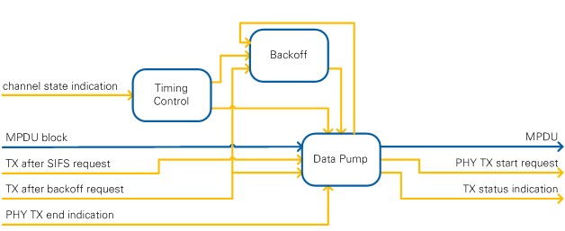
The module MAC TX implements low-level latency critical MAC transmission functionality, i.e. the timing aligned provision of payload data and associated control information to TX PHY. Input to the module are MPDU blocks, which include the MAC header and frame body. These blocks are then extended by the FCS field to form a complete MPDU. For transmission in 802.11ac format, the module generates A-MPDUs by adding delimiter fields and padding to the MPDUs. version 2.0 and 2.0.1 of the 802.11 Application Framework only supports A-MPDUs with a single MPDU. The module supports backoff counting and handles Clear Channel Assessment (CCA) information provided from MAC RX. Furthermore, it ensures correct interframe spacing for the following scenarios:
- SIFS before ACK packet transmission
- DIFS/EIFS before Data packet transmission
- The module implements two transmission types:
- Transmission after backoff Transmission in normal slots using CCA evaluation and backoff counting with application of DIFS or EIFS as needed.
- Transmission after SIFS Transmission at the end of SIFS period without any CCA evaluation. For instance, it is used for the ACK frame transmission.
As shown in Figure 29, the module consists of three major submodules:
- Timing Control
- Backoff
- Data Pump
All three modules are described in the following sections in more detail. Notice that the overall internal structure of MAC TX follows the concept of the IEEE 802.11 SDL specifications. Refer to Section J.5 of [1] for more information about the SDL specifications.
Figure 29: MAC TX block diagram
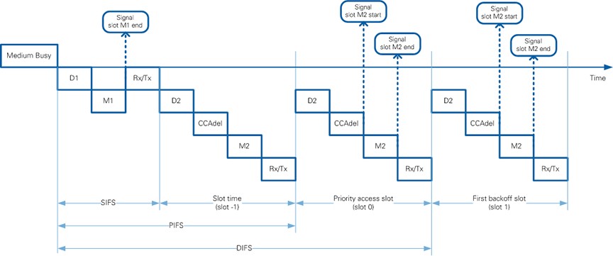
The module Timing Control implements the actual generation of timing information (timing signals) for the transmission part. At startup, a regular slot timing pattern is generated. The pattern consists of two signals, which are also shown in Figure 30:
- Signal slot M2 start Provided to the module Backoff, refers to timing instant of CCA check. The name M2 start and other signal names described below are derived from the identifiers used in Figure 9-14 of [1].
- Signal slot M2 end Provided to the module Data Pump, refers to timing instant of issuing a packet transmission to TX PHY taking into account the processing delay of the TX PHY and RF components.
The Timing Control module consumes timing information from the MAC RX. For frames received with valid length information independent of the actual FCS result, MAC RX provides a reference to the frame end timing to MAC TX. Based on this information, the Timing Control determines the correct interframe spacing and generates timing signals for transmission after SIFS (signal slot M1 end) and transmissions in regular slots after DIFS or EIFS depending on whether the frame reception was completed with FCS pass or fail.
Figure 30: Inter frame timing relationships
The module Backoff performs the backoff procedure as defined in [1] Section 9.3.3. The backoff counter is initialized with the desired backoff value, provided through the TX after backoff request. At the appropriate timing instant within relevant slots, which is indicated to the module with the slot M2 start signal, the CCA information is checked and if the channel is idle, the backoff counter is decremented. If the counter reaches zero, this condition is indicated via the signal backoff done to the module Data Pump.
The module Data Pump coordinates the actual data transmission functionality. The module accepts requests for transmission with or without application of the 802.11 backoff procedure, referred to as transmission after backoff and transmission after SIFS respectively. Those requests are processed based on the timing and backoff information described earlier in this section. The module adds the FCS field to the MPDU blocks to generate complete MPDUs. FCS calculation is done based on IEEE 32-bit CRC as specified in [1] Section 8.2.4.8. In the 802.11ac mode, the module generates A-MPDUs by adding delimiter fields and padding. The MPDUs or A-MPDUs together with associated control information are sent to the PHY SAP TX. The module also provides information about active transmissions to the Backoff module to ensure that this is taken into account during backoff counting. At a given instant of time, only one pending or active transmission request is allowed for transmission after backoff and one for transmission after SIFS. To enable higher level MAC entities to control the data flow to MAC TX accordingly, status information is provided by the MAC TX module.
In addition to the functions described previously, the module MAC TX also provides statistics information. version 2.0 and 2.0.1 of the 802.11 Application Framework provides the following statistics:
- Number of TX after SIFS requests detected
- Number of TX after SIFS requests completed
- Number of TX after backoff requests detected
- Number of TX after backoff requests completed
4.1.2.4 TX Bit Processing
The purpose of the TX Bit Processing module is to generate the signal fields and enqueue the PSDU into the data stream. This stream is then serialized, scrambled, encoded, punctured and interleaved before it is passed to TX I/Q Processing. Its block diagram is shown in Figure 31. The types of the data path and the elements of the control path are listed in Table 10.
Figure 31: TX Bit Processing block diagram
| Module | Output Data Type | Output control information |
| MAC TX | U8 | |
| TX PHY State Machine | U32 | TX bit processing parameter length5 enable scrambler |
| Bit Serializer | Boolean | enable scrambler |
| Scrambler | Boolean | |
| Convolutional Encoder | Boolean array (2 elements) | |
| Puncturer | Boolean | |
| Interleaver | Boolean | packet configuration |
Table 10: TX Bit Processing Data Types and Control Information
The first module in TX Bit Processing is the TX PHY State Machine which encodes the signal fields according to 18.3.4 of [1] (L-SIG), 22.3.8.3.3 of [2] (VHT-SIG-A) and 22.3.4.8 of [2] (VHT-SIG-B). The Data Generator VI furthermore turns PSDU into a sequence of SERVICE field, PSDU data, TAIL, and PADDING for the 802.11a format according to 18.3.5 in [1] or SERVICE field, PSDU data, PADDING and TAIL for 802.11ac format according to 22.3.4.9 in [2] respectively. The Generator outputs are combined using the enable driven stream combiner (EDSC) pattern (see Section 7.1.1). The TX Bit Processing has a head start of two OFDM symbols to have the first bits available when needed by the TX I/Q Processing. This is due to the pre-generation of L-STF (two OFDM symbols) in time domain; the I/Q data of L-STF is stored in a block RAM (refer to Section 4.1.2.6).
Each signal field is generated in one burst. The data bits are generated as one continuous burst per OFDM symbol in dependence on NDBPS. A small FIFO with a four-wire handshake ensures that bytes for at least one OFDM symbol are available. Furthermore, TAIL and PADDING bits are also generated as part of the corresponding burst. In the worst case, the bit processing chain generates bits for up to two OFDM symbols in one burst, which is compensated in a FIFO of the TX IQ Processing Data Assembler.
After the downstream module is the Bit Serializer module, which converts data fields and PSDU data into one bit per cycle. At the start of the module, a FIFO is used to ensure that the module can process the incoming data rate. The maximum number of data bit per symbol NDBPS is 720 (802.11ac, 40 MHz, MCS 9). Because PSDU data is given in bytes, the FIFO must store at least 90 samples.
After bit serialization, scrambling, convolutional encoding, puncturing, and interleaving are applied as described in 18.3.5.5 - 18.3.5.7 of [1] and 22.3.10.4 - 22.3.10.8 of [2]. The scrambler and the encoder must be reset before the first bit of the data field is processed. The Scrambler module is bypassed for signal fields. The Puncturer module serializes the two stream of the convolutional encoder using the puncturing patterns of figure 18-9 and 20-11 of [1]. A FIFO is used on the input of the module since the data rate is higher on the input. The Interleaver applies the BCC interleaver operations, which are defined in Section 18.3.5.7 of [1] and Section 22.3.10.8 of [2]. The write operation into the memory is based on equation 22-77 of [2], which applies the first permutation. The read operation is based on equation 22-82 of [2], which applies the second permutation. Reading is started as soon as all bits of the current OFDM symbol are saved to memory. A double page memory is used, which enables reading and writing at the same time. The output of the Interleaver and the modulation scheme that is used are provided on the output of the TX Bit processing module.
| Module | Output Timing |
| L-SIG Generator | U32 on start of L-SIG processing |
| VHT-SIG-A Generator | 2 U24 on start of VHT-SIG-A processing burstwise |
| VHT-SIG-B Generator | U32 on start of VHT-SIG-B processing |
| Data Generator | NDBPS/8 U32 / OFDM symbol burstwise |
| Bit Serializer | NDBPS bits or array of bits / OFDM symbol burstwise |
| Scrambler | |
| Convolutional Encoder | |
| Puncturer | NCBPS bits / OFDM symbol burstwise |
| Interleaver |
Table 11: TX Bit Processing Transfer Timing
The output timing of the submodules is given in Table 11. All submodules of the TX PHY state machine generate data on the asserted enable signal from the OFDM symbol trigger type module. The modules need up to two U32 words. Starting with the OFDM symbol for the data field, the Data Generator provides the required number of bytes. After the Bit Serializer, NDBPS clock cycles are needed to complete the transfer. The rate ½ convolutional encoder doubles the number of bits but due to the transfer of an array, the number of transfers is not changed. After puncturing, NCBPS bits remain.
Figure 32: TX Bit Processing Latency
The latency of the bit processing chain depends on the format, bandwidth, and MCS. Similar to Table 11, Figure 32 refers to the two corner cases of Non-HT mode with MCS 0 and highest MCS at highest bandwidth. The latency is given for the first subcarrier of the packet. So this is the time the TX bit processing chain needs from start trigger until the first valid bit is provided. Most of the modules have a fixed latency.
The Interleaver must store bits from one complete OFDM symbol. The read operation starts as soon as the last value arrives. NCBPS bits must be read before the last sample is available on the output of the Interleaver. An additional latency of 11 comes from the pipeline stages.
The latency of the FIFOs in Bitserializer and Puncturer are unknown.
4.1.2.5 TX IQ Processing
The purpose of the TX IQ Processing module is to add the training fields and to convert the bits from TX Bit Processing into baseband I/Q samples. The OFDM symbol trigger of the RF loop is used to clock the generation of the OFDM symbols (see Section 3.3.1). The block diagram is illustrated in Figure 33. The data types and control information are listed in Table 12.
Figure 33: TX IQ processing block diagram
| Module | Output Data Type | Output control information |
| TX Bit Processing | Boolean | |
| Create Packet Structure | Field Map Subcarrier Timing TX IQ Processing Parameter | |
| L-STF Assembler | CFX 3.136 | |
| Assembler modules | CFX 2.14 | |
| Channel Duplication | CFX 2.14 | |
| Channel Rotation | CFX 2.14 | |
| IFFT Prescale | CFX 0.16 | |
| Xilinx IFFT | CFX 3.13 |
Table 12: TX IQ Processing Data Types and Control Information
The Create Packet Structure modules creates a timing structure, a field map, and the processing parameters that stay constant along the OFDM symbol. These parameters can include bandwidth, CP length, channel duplication, channel rotation, and tone scaling factor.
The field map controls which field is generated for the current OFDM symbol. Using the EDSC pattern (see 7.1.1) for field generation reduces the latency caused by parallel execution. There is one assembler for each training field, for the pilots, and one for the bit taken from TX Bit Processing module.
TX IQ Processing has to start delivery of IQ data as soon as possible after the TX start request is triggered. Because the IFFT takes about half an OFDM symbol (as described in Section 4.1.2.7), the L-STF is pregenerated in the time domain, and its I/Q data is stored in a block RAM. For each combination of bandwidth and primary subband, a bank is reserved in the memory. Because L-STF is a Non-HT field, you do not need to distinguish between 802.11a and 802.11ac. For 802.11a, an additional bank for DC centered signal exists. Because L-STF is a repeating sequence in time domain with a period of 0.8 µs, you need to store only 64 samples.
The remaining training fields are generated according to Sections 22.3.4.3 (L-LTF), 22.3.4.6 (VHT-STF), and 22.3.4.9 (VHT-LTF) of [2].
The L-DATA and VHT-DATA are built from bits generated by TX Bit Processing modules. The bit stream is buffered in a FIFO that is laid out to buffer up to three OFDM symbols, which are the bit processing head start, the current OFDM symbol, and the last OFDM symbol, if filled with padding. Besides applying the correct modulation, the module also rotates VHT-SIG-A2 according to 22.3.8.3.3 in [2].
The pilot tones are inserted according to 22.3.10.10 of [2] using the information from the field map.
After the assembler modules, the channels are duplicated and rotated according to Sections 22.3.4.x and 22.3.7.5 of [2]. Here, the Create Packet Structure modules ensure correct settings for handling channel duplication and rotation.
Next downstream module is the IFFT prescale. This module applies tone field scaling according to 22.3.7.4 of [2] to ensure that the time domain power of VHT modulated fields does not exceed the time domain power of pre-VHT modulated fields (each summed over all transmit channel). The scaling factor is determined in the Create Packet Structure module and depends on bandwidth and field type (refer to table 22-8 of [2]).
The last module is the IFFT, which is a wrapper around the Xilinx IFFT core. It contains a 256-point IFFT operation using Radix 4, Burst I/O architecture similar to the RX IQ processing. In addition, the configuration input is used to enable cyclic prefix insertion by the core. The core configuration settings, such as this input, are dynamic and are provided parallel to the first sample of each OFDM symbol. A small FIFO is placed before the IFFT input to compensate the longer execution time due to guard interval GI2 of L-LTF-1. The IFFT output is shifted in frequency using a toggling negation due to the implementation on the FPGA. The fixed point format on the output is CFX 3.13 based on the requirements of Section 3.3.3.3.
Figure 34: TX IQ Processing Latency
There are two paths for latency in TX I/Q processing. One goes for the precalculated samples of the L-STF in the time domain. This path has only a latency of five cycles, which allows the PHY to ensure a packet starts at the interface to the RF when it is trigger inside the PHY. The second path goes for all the other symbols that are created using the path shown in Figure 34. The FFT latency is smaller than reported by the Xilinx core because the reported value includes loading of all 256 samples. During the packet, the FFT executes and unloads samples in 616 clock cycles after the last sample arrived. The remaining clock cycles per OFDM symbol are used to transfer data from the input FIFO to the FFT core. By the time the last sample is available on the input, the FIFO is empty and it is passed to the core as fast as possible. The delay of the FIFO is unknown. All other modules have a fixed latency.
4.1.2.6 Timing
The overall timing of the TX chain including TX Bit processing and TX IQ Processing is shown in Figure 35 for packets in 802.11ac format. The timing works similarly for 802.11a packets. Time is represented on the horizontal axis. On the vertical axis only a couple of module outputs are chosen that are important or change the transfer timing. The colored rectangles correspond to the data values of one OFDM symbol. The size and the placement among the time axis are related to the latencies and transfer timings of the modules. The black arrows show important control signals inside the processing chain and between PHY and MAC. The arrows are based on the timing information.
Figure 35: TX PHY Timing for 802.11ac packets
Figure 35 shows the timing of the transmitter for an 802.11ac packet. The RF transmission starts with the start of packet trigger that is given with the start of the first OFDM symbol. This is possible because the L-STF is unloaded from memory in time domain. The latency is only a few cycles. In parallel, the bit processing starts with the encoding of bits for the L-SIG and the I/Q processing starts assembling the L-LTF. The head start of four symbols for the bit processing and two symbols for the IQ processing is kept during the packet generation. This design ensures that all samples arrive in time for I/Q processing and RF.
Assembling the bits takes only a few cycles. Bit insertion when the code rate is applied in convolutional encoding and puncturing causes the chain length of valid samples to increase at the end of TX Bit processing. The samples leave the bit processing as a burst because the interleaver handles data in groups NCBPS .
The assemblers in RX IQ Processing module append training fields and add pilots to the fields generated by TX Bit Processing module. Each OFDM symbol will contain 256 I/Q samples. The IFFT transforms this I/Q data into time domain and adds guard interval. This transformation takes 360 cycles plus FIFO delay.
In case of an invalid TX Request, there is no packet generation at all and the PHY TX Request handler generates the TX end indication immediately.
4.1.3 RF
The digital downconversion (DDC) and digital upconversion (DUC) modules are based on the PXIe Streaming project templates of USRP and NI 579X. Their block diagrams are shown in Figure 36 and Figure 37. In the downconversion path, a DC Offset Correction module is present to estimate and compensate the residual DC offset from the RX LO. This module mitigates the impact to the autocorrelation computation within the Synchronization block. The DC Offset Correction module estimation uses an average over 512 samples. After each averaging window, the LSB of the correction value is increased or decreased. Over time, the correction value is approaching the DC offset iteratively.
Figure 36: DDC block diagram
Figure 37: DUC block diagram
The latencies of DDC and DUC are given in Figure 39 and Figure 39. The Fractional Decimator and Interpolator latencies depend on the ratio of clock rate versus sample rate. Since USRP devices and FlexRIO devices have different clock rates, the DDC has a target-specific latency. The latency for the DUC remains the same for both target types.
Figure 38: DDC latency
Figure 39: DUC latency
The analog parts of the device and FPGA logic that are not presented on the block diagram add latency to the RF path. Those can be measured using RF loopback and the Streaming project templates for the specific target. The results are listed in Table 13.
| USRP RIO 40 MHz BW (Data clock = 120 MHz) | USRP RIO 120 MHz or 160 MHz BW (Data clock = 200 MHz) | FlexRIO / FAM (Data clock = 130 MHz) | |
| DDC | 57 clock cycles ~ 0.48 µs | 72 clock cycles ~ 0.36 µs | 59 clock cycles ~ 0.45 µs |
| DUC | 40 clock cycles ~ 0.33 µs | 50 clock cycles ~ 0.25 µs | 40 clock cycles ~ 0.31 µs |
| Others (ADC, DAC, ...) | 100 clock cycles ~ 0.83 µs | 50 clock cycles ~ 0.25 µs | 115 clock cycles ~ 0.88 µs |
| RF round trip time | 197 clock cycles ~ 1.64 µs | 172 clock cycles ~ 0.86 µs | 214 clock cycles ~ 1.65 µs |
Table 13: RF latency
4.2 Host
The host is a sample application that covers all important features of the 802.11 Application Framework. This covers configuration of the FPGA target, exchanging payload data and monitoring the system status.
4.2.1 Host Architecture
The host is split into six loops covering the jobs of configuration, data exchange, and status display (refer to Figure 40). The initialization of the system and the cleanup are done on the upper left and upper right of the block diagram respectively. The system status is passed around with the help of a session cluster that stores all handles to devices and queues used in the host application.
There are a few queues used to buffer and pass payload and status information around the system (refer to Table 14). All queues are part of the session cluster.
| Queue | Purpose |
| stop | Synchronizes shutdown of all loops in case an error occurred or the stop button was pressed. |
| send | Buffer data that should be transmitted to the target. |
| receive | Buffer payload received from the target. |
| receive throughput | Stores information about received payload size and timestamps (used for throughput graph display). |
Table 14: Message Queues used in Host Application
The loops for data transmission between target and host as well as between host and UDP ports run without throttling to achieve the maximal possible throughput. The loops for configuration and status display run every 100 ms to enable a responsive system. The loop to display events, constellation, channel estimation, and spectral plots runs at a slower rate (every 250 ms), as it consumes a lot of processing power.
Figure 40: Host schematic block diagram
4.2.2 System Configuration
The parameters for system configuration are split into three groups, and they are ordered on the front panel from top to bottom such as the following:
Group 1: Parameters can only be changed at system start, which can be found on the upper right. Those are the RIO device and reference clock.
Group 2: Parameters can only be changed while the station is off, which can be found above the gray line in each tab. Those parameters are the operation mode, the carrier frequency, the power level, and the TX and Rx port number.
Group 3: Parameters can be changed at any time such as the subcarrier format, the MCS, data source options, etc. They can be found below the gray line in each tab.
For a detailed description of each parameter, refer to the HTML documentation included inside the project files tab [5].
4.2.3 Gain Control
The gain control mechanism on the host allows the user to switch between a manual gain configured on the front panel and the AGC implemented on the FPGA as described in Section 4.1.1.3.
Some AGC settings like the threshold level that enables the gain control and the threshold levels for the four gain steps can be configured from the host. These settings can be found as constants in the 802.11 Configure AGC Registers subVI.
5 Performance
5.1 TX EVM
The TX error vector magnitude (EVM) is -35 dB or better for the peak TX power level settings as given in Table 15. Measurements have been taken using NI WLAN Analysis Soft Front Panel Rel. 14.0 and the PXIe-5644R VST.
| USRP-2942 | USRP-2943 | 5791 | ||||
| Frequency | Min. | Max. | Min. | Max. | Min. | Max. |
| 2.45 GHz | -8 dBm | 19 dBm | -6 dBm | 21 dBm | -24 dBm | 7 dBm |
| 5.85 GHz | - | - | -18 dBm | 10 dBm | - | - |
Table 15: Minimum and maximum peak TX power level for EVM = -35 dB or better
5.2 Minimum RX Sensitivity
Minimum RX sensitivity for MCS 0 (BPSK, 1/2) and MCS 7 (64 QAM, 3/4) is presented in Table 16. The measurements follow the rule given in Section 18.3.10.2 of [1]:
1. The packet error ratio (PER) shall be 10% or less when the PSDU length is 1,000 octets.
2. The minimum input levels are measured at the antenna connector.
Measurements have been taken using NI WLAN Generation Soft Front Panel Rel. 14.0 and the PXIe-5644R VST.
| USRP-2942 | USRP-2943 | NI 5791 | ||||
| Frequency | MCS 0 | MCS 7 | MCS 0 | MCS 7 | MCS 0 | MCS 7 |
| 2.45 GHz | -81 dBm | -71 dBm | -84 dBm | -72 dBm | -74 dBm | -65 dBm |
| 5.85 GHz | - | - | -75 dBm | -67 dBm | - | - |
Table 16: Minimum RX sensitivity
5.3 Throughput
Throughput considering DATA-ACK sequence, backoff value of 15, and different packet sizes is given in Table 17.
| 802.11a | 802.11ac | ||
| VHT20 | VHT40 | ||
| Packet size (bytes) | MCS 7 | MCS 8 | MCS 9 |
| 2304 | 30.9 Mb/s | 34.3 Mb/s | 45.8 Mb/s |
| 4000 | 37.7 Mb/s | 45.1 Mb/s | 67.0 Mb/s |
Table 17: Throughput for DATA-ACK sequence in 802.11a, 802.11ac VHT20 and VHT40
6 Conclusion
The LabVIEW Communications 802.11 Application Framework provides a real-time 802.11 implementation running on NI SDR hardware. This framework enables you to focus on a specific area of research by utilizing the existing link and only making changes or additions where desired.
Because of the flexibility of LabVIEW and the modularity of the framework, you can easily exchange portions of the design for prototyping new algorithms for future wireless systems. In addition, LabVIEW's native interface between the host and the FPGA means that the design can be partitioned to profit from the parallel execution on the FPGA as well as calculations on the host.
The 802.11 Application Framework provides a comprehensive set of features. The overall architecture described in Section 3 allows to extend the 802.11 Application Framework towards features such as support for MIMO, VHT 80 MHz bandwidth mode, 802.11p PHY extensions, DCF functionality (retransmissions, request-to-send / clear-to-send (RTS/CTS)), QoS support or 802.11p MAC extensions.
This 802.11 Application Framework offers a variety of starting points for wireless research and prototyping. Start now by downloading an evaluation copy of LabVIEW Communications at www.ni.com/labview-communications.
Questions? Email us at labview.communications@ni.com.
7 APPENDIX
7.1 Design Pattern
7.1.1 EDSC
The enable driven stream combiner is used to combine information from different sources into one stream. You can use the EDSC to map different fields into the frequency domain of one OFDM symbol. The idea is illustrated in Figure 41 for 3 computational VIs.
Figure 41: Enable driven stream combiner
There is a single Stream Generation VI that generates control information for the computational VIs. This comprises an enable signal for each computational VI. Only one of these enable signals is asserted at a given time. The asserted enable signal defines the structure of the stream that should be generated. Afterwards, an unlimited number of computational VIs provide their data on the output whenever the corresponding enable signal is asserted. When the enable signal is not asserted, the output is zero. Because of this constraint, a simple OR gate can be used to combine the streams.
There is no throttle control mechanism in this design pattern. The assumption is that the computational module can always provide data when the enable signal is asserted. This has to be ensured by the stream generation before start.
If the computation of one of the VIs require pipelining, the other paths between Stream Generation VI and the OR gate have to be delayed to equalize path latencies. Since the output of the computation usually has a wider bit width than the enable signal, it is recommended to add the delay before the computational modules.
7.2 Protocols
7.2.1 Event FIFO
The 802.11 Application Framework utilizes a target-to-host FIFO. It is reserved for event messages, that are passed between modules on the target. The message must be small in size. All information must fit into a 64-bit integer, where eight bits are reserved for the event ID. These IDs have to be consecutive, unique numbers starting with zero.
Figure 42: Event Arbitration on FPGA
The arbitration of the FIFO events in one clock domain on the FPGA is illustrated in Figure 42. Since the timestamp is added in the Event to FIFO VI, the order of the events in the target to host FIFO is not related to the correct order of arrival on the FPGA. One event that occurs burstwise needs multiple arbitration rounds to get written to the FIFO. These multiple arbitration rounds increase the time difference between arrival and timestamp value.
There is an event specific conversion VI that creates an U64 integer from the event information and contains the condition for writing an event. If the condition is met, the U64 value is written to a local FIFO. This FIFO ensures that there is no loss of events because of the arbitration for the target-to-host FIFO. The conversion VI also contains the unique ID for this event. It is available on the output of this VI and is part of the U64 word.
The local FIFO reference and the event ID are provided to a common Event to FIFO VI that has to be instantiated once per event. It contains the arbitration logic for the target-to-host FIFO. The value of the round robin counter is checked against the given event ID. If a match is detected, two U64 words are written to the target-to-host FIFO. The first word contains the timestamp while the second word is the event data read from the local FIFO reference. Since the event IDs are unique, there is only one instance of the Event to FIFO VI writing to the FIFO.
Due to the round robin scheduling and two words per event, the event FIFO throughput is limited. The rate for each event has to be lower than two times the total number of events. Events can appear at a higher rate as long as the local FIFO is able to store those values.
Since the timestamp is added in the Event to FIFO VI, the order of the events in the target-to-host FIFO is not related to the correct order of arrival on the FPGA. One event that occurs burstwise needs multiple arbitration rounds to get written to the FIFO. Multiple arbitration rounds would increase the time difference between arrival and timestamp value.
7.2.2 ICP
ICP stands for Interprocess Communication Protocol. The Application Framework uses this protocol to transfer data from host to target and vice versa. The idea is to send messages with fixed structure and varying length over a channel that is able to transmit a stream of bytes such as the DMA FIFOs. The design is very simple and it is open for future enhancements, such as multiplexing different structures in the same stream or recovering from FIFO overflow with the help of a sync word. In the current implementation, all structures start with a length field of four bytes in network order encoding the length of the overall structure excluding the length field itself. The Application Framework uses two structures to transfer data to Target TX (Figure 43) and to send data received by the Target RX (Figure 44).
Figure 43: ICP TX Format
The ICP TX structure serializes the TX Request. The format and MCS are mapped to two bits and MCS is mapped to 4 bits. Power Level is not used in the current design. Scrambler Seed must not be zero. The TX Request is followed by the MAC payload.
Figure 44: ICP RX Format
The ICP RX structure serializes the RX indication. The Decoding status contains the following bits:
- FCS result CRC check succeeded
- Header recognize done header recognize was finished
- Header recognize error header contains a decodable frame subtype (current designs supports DATA and ACK)
- Address matching the destination MAC address of the packet equals the device MAC address
- Valid Indication is valid
The RX indication is followed by the MAC payload (MPDU without header information)
7.3 Viterbi Decoder Implementation
The Viterbi decoder core is capable of handling convolutional decoding for the 802.11 standard as well as for the control channel of the LTE standard. This can be configured via the operation mode interface.
The 802.11 standard defines convolutional encoding as forward-error correction coding in all transmission fields. The corresponding receiver in the 802.11 Application Framework uses a Viterbi decoder implementing the Maximum Likelihood Sequence Estimation (MLSE) algorithm based on softbit input. A rate ½ convolutional code with a constraint length of 7 and the code polynomials [133, 171] is used. It is terminated with a sequence of zeros to reset the encoder to the all zero state after encoding.
7.3.1 Design considerations
For the 802.11 Application Framework, the Viterbi implementation has to enable a throughput of 180 Mbit/s at a clock rate of 250 MHz. Additionally, the latency of the block must be less than 2 µs to meet the SIFS timing. In the 802.11 standard, the code blocks of signal fields are very short compared to the large data field code blocks.
7.3.2 Operation Principle
The Viterbi decoder consists of the three modules: branch metric computation, path metric accumulation & survivor selection, and traceback handling for actual decoding, as shown in Figure 45.
Figure 45: Viterbi operation principle
In the branch metric computation, the received softbits are multiplied by the hypotheses to form the state transition metric. This branch metric is used to update the path metric of all 64 states and calculate the surviving path. The corresponding Boolean bit value is stored in the traceback memory. After a certain amount of iterations - the traceback length - the maximum path metric is determined and from its state the traceback memory is evaluated backward to decode bits in history along the most likely path in the Trellis.
The metric computation is running in a streaming mode and fills the traceback buffer continuously, but the actual decoding with evaluation of the traceback memory is initiated only every traceback length time instances. Hence, it is necessary to flush the metric computation with artificial softbits to enable traceback evaluation and decoding for the last bits of a code block as well.
7.3.3 Interface
The Viterbi core is capable of handling one bit per clock cycle. There is no handshaking implemented in the direction of upstream and downstream modules. The modules must be capable of handling continuous data streaming. The input valid and output valid signals are used to indicate valid samples.
The data bit? flag is aligned to the data. This Boolean is not used by the core but is delayed parallel to the processing. It can be used to distinguish data bits and flushing bits, which are required to decode the last bits of the code block.
The incoming data shall be given as Log-likelihood Ratios as defined in Equation 8. Based on the code rate, two code bit inputs ( code bit 0 and code bit 1) must be used. The third code bit input (code bit 2) remains unused for rate 1/3 convolutional coding in the 802.11 Application Framework. However, it is used for the LTE Application Framework. The fixed-point format is FXP4.1. Based on the quotient a strong probability for a transmitted symbol 

Equation 8: Log-likelihood Ratios
The output of decoded bits is given as a Boolean. The mapping from Booleans to symbols is done such that a false equals 1 and true equals -1 (see Equation 9).
Equation 9: BPSK Mapping
The operation mode must be set to constant 802.11 to work within the 802.11 Application Framework. The traceback length defines the minimum number of states the Trellis is continued before decoding the current state. The valid range is 1 to 127. This value must be set to a constant as well.
7.3.4 Implementation
The block diagram of the implementation is illustrated in Figure 46.
Figure 46: Viterbi block diagram
The branch metric computation is implemented with simple sign changes and additions. This submodule has an Application Framework specific implementation corresponding to the code rate. For the 802.11 Application Framework only code bit 0 and 1 are used since the encoder has code rate 1/2. Code bit 2 is ignored. Hence, the output of the branch metric computation yields 4 valid values only. The subsequent modules are independent of the code rate.
In the path metric computation, often named Add-Compare-Select in literature, for every state from the 64 states, the path metric values of the two preceding states are updated with the corresponding branch metrics and the larger value of the resulting values is stored as the new path metric for this state. At the same time, the result of the comparison is stored as a Boolean value to mark the more likely state transition of the surviving path. The outputs of the submodule are a new 64 element vector of path metrics and a 64 element Boolean vector of survivor paths for every bit vector input.
The operation mode selector is used to set the appropriate initial value of path metrics and the correct selection of the branch metric element for the state transition (one out of the valid four). Since the 802.11 standard defines Trellis termination with Zeros, the start vector of path metrics gives a competitive edge for the zero state over all other states.
The path metric computation submodule does not have a reset. Thus at the end of a code block, the path metric memory must be similar to the described start vector to allow continuity of code block handling. This is achieved by flushing appropriate softbits (see Section 7.3.2). For the 802.11, Trellis termination softbits representing a high probability of transmitted Zeros are flushed (strong Zeros). If the path metric vector does not already have the highest value for state 0, flushing will take care of it.
Normalization of the path metric values is used to avoid infinitively growing values and restrict the bitwidth. Since only the difference between path metrics is of interest but not their absolute value, normalization does not influence the decoding result. The process is stretched to two clock cycles. In the first clock cycle, all path metric values are checked versus a threshold before they are written to a memory. In the second clock cycle based on the threshold comparison, a constant value is subtracted from the branch metric prior to updating the path metrics.
The survivor path is written to two traceback memories. After traceback length samples, one of the two traceback paths is triggered. The most probable state at this point in time is the one with the largest path metric value. Its index is provided by the Find Best State module. Starting from this state, the Traceback Calculation module recursively calculates the previous state based on the survivor path vectors from the traceback memory. The decoded bit is derived from the LSB of this survivor state.
It is worth mentioning that the first decoded bits of the survivor path show lower reliability than later elements in the traceback. Thus, the first half of the bits is discarded. The order of the remaining decoded bits must be reversed because the traceback memory is evaluated backwards. Both operations are done in the Bit Reordering module.
In the last step, the outputs of the two traceback chains are combined to a final decoded sequence, which is available on the output.
7.3.5 Timing
The timing of the Viterbi decoder is shown in Figure 47. It is independent of the chosen operation mode but it depends on the traceback length. As described in Section 7.3.4, there are two traceback chains which are illustrated in different colors. The horizontal axis represents the time. A scale with multiples of traceback length clock cycles is visible on the top as a reference. The timing diagram assumes that there is a valid input in each clock cycle. The traceback memory is empty at the beginning.
Figure 47: Viterbi timing
All input data is processed in the branch and path metric calculation. This calculation adds two cycles of latency before storing the data to the traceback memory. The first traceback memory is read as soon as two times traceback samples are written. The second traceback chains starts another traceback samples delayed. The Traceback Calculation module just adds one cycle of latency. At the output of the Bit Reordering module, only the second half of the samples is declared as valid after two times traceback length elements have been written. The outputs of both traceback chains are combined to a continuous output stream.
If the input is not valid at each clock cycle, the input pattern is kept until the traceback memory input. Afterwards, the traceback decoding and bit reordering are performed burst wise. In this case, the latency of every wait cycle on the input will increase the latency for the first code block input by one cycle. NI recommends flushing the Viterbi core with a continuous stream to have the minimum latency for the end of the code block.
This concept results in a decoding latency of four times the traceback length (plus 13 clock cycles processing time). During two times the traceback length of the traceback buffer is written, and during another two traceback lengths the evaluation and decoding take place. The evaluation in chunks of two times the traceback length makes it necessary to flush the Viterbi decoder with exactly the same number of input softbit triples. The latency of each module is summarized in Figure 48.
Figure 48: Viterbi latency
7.3.6 Resource Usage
The Viterbi implementation occupies the FPGA resources listed in Table 18.
| Operation mode | 802.11 |
| LUTs | 4189 |
| Registers | 1990 |
| Block Ram (36k) | 2 |
Table 18: Viterbi resource usage
7.3.7 Throughput
The throughput in MS/s is equal to the clock rate in MHz since the core is capable of handling one sample per each clock cycle. Synthesis of the core is successful up to a clock rate of 300 MHz.
8 Abbreviations
| Abbreviation | Meaning |
| ACK | Acknowledgement |
| ADC | Analog Digital Converter |
| AGC | Automatic Gain Control |
| A-MPDU | Aggregated MPDU |
| BLER | Block Error Rate |
| CCA | Clear Channel Assessment |
| CTS | Clear-to-send |
| CSMA/CA | Carrier Sense Multiple Access with Collision Avoidance |
| CW | Continuous Wave |
| DAC | Digital Analog Converter |
| DIFS | Distributed (coordination function) Interframe Space |
| DCF | Distributed Coordinate Function |
| EDSC | Enable Driven Stream Combiner |
| EIFS | Extended Interframe Space |
| EVM | Error Vector Magnitude |
| FAM | Frontend Adapter Module (RF module) |
| FCS | Frame Check Sequence |
| ICP | Interface Communication Protocol |
| IFS | Inter Frame Spacing |
| LUT | Look-up Table |
| LLR | Log-likelihhod Ratio |
| MAC | Medium Access Control Layer |
| MCS | Modulation and Coding Scheme |
| MPDU | MAC PDU |
| MSDU | MAC Service Data Unit |
| MSB | Most Significant Bit |
| NACK | Negative Acknowledgement |
| NDP | Null Data Packet |
| OFDM | Orthogonal Frequency-Division Multiplexing |
| PDU | Protocol Data Unit |
| PHY | Physical Layer |
| PIFS | Point (coordination function) Interframe Space |
| PLCP | PHY Layer Convergence Protocol |
| PN | Pseudo Noise |
| QAM | Quadrature Amplitude Modulation |
| RF | Radio Frequency |
| RX | Receive |
| RTS | Request-to-send |
| SDL | Specification and Description Language |
| SDU | Service Data Unit |
| SIFS | Short Interframe Space |
| SISO | Single Input Single Output |
| TX | Transmit |
| UDP | User Datagram Protocol |
| VHT | Very High Throughput |
9 Bibliography
| [1] | IEEE, "Part 11: Wireless LAN Medium Access Control (MAC) and Physical Layer (PHY) Specifications," 2012. |
| [2] | IEEE, "Part 11: Wireless LAN Medium Access Control (MAC) and Physical Layer (PHY) Specifications; Amendment 4: Enhancements for Very High Throughput for Operation in Bands below 6 GHz," 2013. |
| [3] | IEEE, User guide for 802.11ac waveform generator, IEEE 802.11-11/0517r6, 2011. |
| [4] | T. M. Schmidl and D. C. Fox, "Robust Frequency and Timing Synchronization for OFDM," IEEE Transactions on Communications, vol. 45, no. 12, pp. 1613-1621, 1997. |
| [5] | "802.11 Application Framework Getting Started Guide," National Instruments, 2015. |
| [6] | 3rd Generation Partnership Project, "TS 36.212 V10.0.0 Multiplexing and channel coding". |


