What Clock Error Means to Your Measurement System
Overview
Contents
- Role of the Clock
- Components of Clock Error
- Effects of Clock Error Components
- Methods of Improvement
- Improving System Clock Error
- Conclusion
- Additional Contributors
Role of the Clock
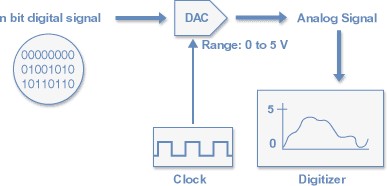
The clock plays a critical role in almost any measurement system. With hardware-timed measurements, the clock controls when the samples or updates occur. You might choose a hardware-timed measurement to achieve a more consistent time interval between samples or updates than you would have if you relied on software to time your measurements. Take, for example, the case of characterizing a digital-to-analog converter (see Figure 1). There are three basic parts to this application -- the digital data stimulus to the digital to analog convertor (DAC), the clock signal, and the digitizer to acquire the analog waveform generated by the DAC. The DAC clocks in a new n-bit word with every rising edge of the clock signal to generate a point in the analog waveform. If the clock signal to the DAC has error, then the analog signal generated by the DAC reflects that error.

Figure 1. DAC Characterization
Components of Clock Error
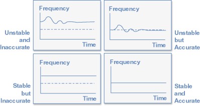
A clock is typically generated by a crystal oscillator, and no oscillator perfectly generates the specified frequency. There are three main components of clock error -- accuracy, stability, and jitter. The clock accuracy describes how well the actual frequency matches the specified frequency. Clock accuracy might be affected by factors such as the quality of the oscillator crystal and how the oscillator was assembled. The clock stability describes how well the oscillator frequency resists fluctuations. The dominant factor that affects stability is a variation in temperature, though aging over time, supply voltage, shock, vibration, and capacitive load that the clock must drive can all affect the clock stability. Jitter refers to small variations in the period of the clock from one edge to the next, and each additional hardware component on the measurement device adds jitter. Figure 2 illustrates the effects of clock accuracy and stability.

Figure 2. Effects of Clock Accuracy and Stability
In each of the diagrams, the dotted line represents the specified, desired frequency, and the solid line represents the actual frequency generated by the oscillator. The upper-left diagram shows an inaccurate and unstable clock; the actual frequency is not centered around the desired frequency, and it changes with respect to time. The upper-right diagram shows an accurate but unstable clock; the actual frequency is centered around the specified frequency but still changes with time. Conversely, the lower-left diagram shows a clock that is inaccurate but stable; the actual frequency is not centered about the desired frequency, but the output frequency from the oscillator does not change over time. A perfect oscillator would generate a frequency like that presented in the lower-right diagram, where the clock is accurate about the desired frequency and does not change with time.
Realistically, if you zoomed in on each diagram, you would see small changes in output frequency from one sample to the next. This apparent noise in the actual frequency generated by the oscillator would represent clock jitter.
Effects of Clock Error Components
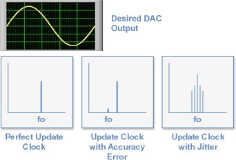
Assume that the DAC is producing a sine wave of a certain frequency. With a perfect update clock, the frequency domain result would be a single impulse at the fundamental frequency (see Figure 3). If the update clock is inaccurate, then the actual frequency output from the DAC is offset from the desired frequency. If the update clock is accurate but contains jitter, then the output of the DAC contains several frequency components other than the desired fundamental frequency. To illustrate the effects of stability, you would need to examine the frequency domain over time and see how the frequency output of the DAC changes over time.

Figure 3. Effects of Clock Error
Methods of Improvement
The clock error is determined by the measurement hardware you choose. To improve your clock error, check the clock error specifications for your device and check the type of oscillator used on your device. Two common types of oscillators are voltage-controlled and oven-controlled oscillators. With a voltage-controlled oscillator (VCXO), the device tunes the output frequency by applying a DC voltage to the oscillator.
With an oven-controlled oscillator (OCXO), an applied voltage controls the output frequency, but an onboard oven maintains a constant internal temperature inside the oscillator. Because the primary contributor to clock instability is temperature variation, controlling the temperature inside the oscillator dramatically increases the clock stability and therefore, greatly improves the overall clock error. By using a device with an OCXO, you can often improve your clock error by a few orders of magnitude.
You can also improve the error from your oscillator by periodically calibrating the timing components of your measurement device. The recommended period between calibration is one year, but you can shorten that period to six months or ninety days depending on the timing precision your application requires. Visit ni.com/calibration for recommended calibration procedures.
Improving System Clock Error
You can improve your overall system clock error by sharing a precision clock source among multiple devices in PXI. If you install a PXI device with a low clock error, such as a device with an oven-controlled oscillator, in the PXI star trigger slot (slot 2) and choose devices that implement phase-locked loop (PLL) circuits, then the PXI devices with PLL circuits can take advantage of the high-precision clock of the device in the star trigger slot. A phase-locked loop is a circuit that compares two clocks -- a reference clock and the output of a VCXO.

Figure 4. Phase-Locked Loop
The PLL compares the two clocks and divides the two frequencies to attain a common frequency. For instance, if the PLL is locking a 15 MHz VCXO clock to a 10 MHz reference clock, it may divide the 15 MHz clock by 15 and the 10 MHz clock by 10. Then, it compares the phase and frequency of the two derived 1 MHz clocks and generates a 1 MHz pulse train. The closer matched the two clocks are in frequency and phase, the narrower the pulse widths of the generated 1 MHz pulse train. The pulses are fed to a low pass filter that delivers a DC voltage at its output based on the width of the pulses at its input. This DC voltage is applied to the VCXO to control the output frequency from the VCXO. The PLL works to adjust the DC voltage to minimize the width of the pulses, and to make the frequency and phase of the clock derived from the VCXO match the clock derived from the reference clock. If your measurement devices include phase-locking circuitry, then the device clock inherits the properties of the reference clock in the PLL. If you supply the devices with a high-precision reference clock, then your other phase-locking devices can take advantage of that high-precision clock throughout your PXI measurement system.
Conclusion
Understanding the components of clock error allows you to better understand your measurements. No measurement system is free of clock error, but there are some steps you can take to minimize the clock error per measurement device or throughout your measurement system. You can choose measurement devices with high-precision oscillators like an OCXO, and choose measurement systems like phase-locking devices in PXI that can share the clock from that high-precision oscillator. Periodic timing calibration of your measurement devices also minimizes the clock error from their oscillators. By understanding the implications of clock error and implementing some of these methods, you can achieve the timing precision required in your measurement application.
Additional Contributors
June Zhe received her Bachelor of Science for Electrical Engineering from Rensselaer Polytechnic Institute. Currently, she is a Product Support Engineer in the Digital and Timing group at National Instruments. Her areas of expertise include customer support and usability of digital and counter/timer products.
Cory Wile received his Bachelor of Science for Electrical Engineering from the University of Texas at Austin. Currently, he is a Hardware Design Engineer in the Digital and Timing group at National Instruments. His areas of expertise include counter/timer products, microprocessors, VHDL design, and device production tests.