Industrial DIO Boards (Output) Signal Connections and Common Causes of Damage
Overview
This document describes the different signal connection schemes that should be adopted while working with NI PCI/PXI-651x 30 V Bank Isolated Industrial DIO boards with high current outputs. This document defines terminology such as sourcing current and sinking current and relates these definitions to your applications using the NI 651x boards. It also provides the pinouts for all the NI 651x boards (with output lines) coupled with examples related to the proper field wiring signal connections. Finally, it describes the main causes for damage to these boards and how to avoid these issues.
Contents
- Defining Sourcing and Sinking for Digital Outputs
- Signal Connections
- Pinouts
- Common Causes of Damage to the Outputs
Defining Sourcing and Sinking for Digital Outputs
The output lines on these boards can either source or sink current to an actuator (or a sensor) depending on the type of actuator. Therefore, different signal connection schemes are required for proper operation.
- Sourcing: A sourcing device provides the power or a positive potential. Sourcing devices "push" the current through the load to ground. Terms used to describe sourcing devices include PNP, Open Emitter, Normally Low, and IEC Positive Logic.
The NI PCI-6512, PCI-6514, PCI-6516, PCI-6518, PXI-6512, and PXI-6514 (even-numbered NI 651 x devices with outputs) are few of the NI DIO devices that have sourcing digital outputs.
- Sinking: A sinking device provides a path for the current to ground and is not responsible for powering the device. Terms used to describe sinking devices include NPN, Open Collector, Normally High, and IEC Negative Logic.
The NI PCI-6513, PCI-6515, PCI-6517, PCI-6519, PXI-6513, and PXI-6515 (odd-numbered NI 651 x devices with outputs) are a few of the NI DIO devices that have sinking digital outputs.
For both sourcing and sinking NI 651 x devices, the output port requires an external power supply to operate. The voltage from this power supply is regulated and passed to the 30 V bank isolated output driver called the Darlington Driver.
For more information on these concepts, refer to Digital I/O Sinking and Sourcing.
Signal Connections
Sourcing
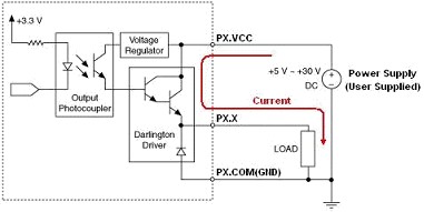
Figure 1: Sourcing Signal Connections
For devices with current sourcing capabilities, notice how the Darlington Driver is involved in sourcing the current that is flowing through the load.
Sinking
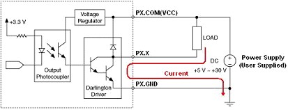
Figure 2: Sinking Signal Connections
For devices with current sinking capabilities, notice how the Darlington Driver is involved in sinking the current that is flowing through the load.
Pinouts
Sourcing NI PCI/PXI-6512/6514/6516/6518
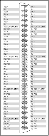 | 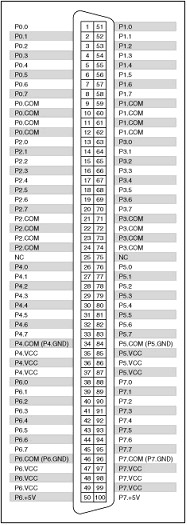 |
Figure 3(a): NI 6512 Pinout
| Figure 3(b): NI 6514 Pinout
|
Figure 3(a and b) shows the pin configuration for the NI 6512 and NI 6514. Please refer to Figure 1 in conjunction with Figures 3a and 3b to conceptualize the actual load connections. Notice that the pinouts for the two devices are different because of the fact that the NI 6514 also supports digital input lines
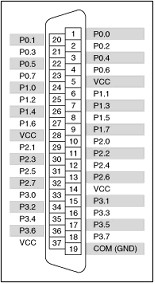 | 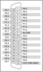 |
Figure 4(a): NI 6516 Pinout
| Figure 4(b): NI 6518 Pinout
|
Figure 4(a and b) shows the pin configuration for the NI 6516 and NI 6518. These devices have lower channel counts than the NI 6512 and NI 6514, and support a 37-pin connector instead of a 100-pin connector.
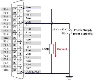
Figure 5: Actual Connections for a Sourcing Output Device.
Figure 5 illustrates the actual connections that would be required to drive a sinking load using one of the sourcing devices. The pinout for the NI 6516 has been used for reference and the signal connections would be similar for other sourcing devices.
Sinking NI PCI/PXI-6513/6515/6517/6519
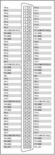 | 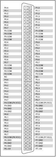 |
Figure 6(a): NI 6513 Pinout
| Figure 6(b): NI 6515 Pinout
|
Figure 6(a and b) shows the pin configuration for the NI 6513 and NI 6515. Notice how the pin functions change for a sinking and a sourcing output device.
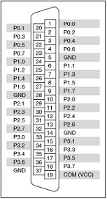 | 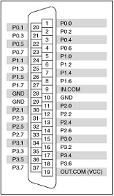 |
Figure 7(a): NI 6517 Pinout
| Figure 7(b): NI 6519 Pinout
|
Figure 7(a and b) shows the pin configuration for the NI 6517 and NI 6519. These devices are similar to the NI 6513 and NI 6515 in operation, respectively, and differ in the number of available digital lines and the device mating connector.
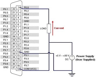
Figure 8: Actual Connections for a Sinking Output Device.
Figure 8 illustrates the actual signal connections that would be required for connecting a sourcing load to a sinking device. The pinout for the NI 6517 has been used for this illustration and the connections would be similar for other sinking devices.
Common Causes of Damage to the Outputs
When used properly (within specifications), the NI 651 x devices are powerful products that provide isolation, high current drive, and up to 30 V digital output signaling. Following are some common misuses that can cause damage to the device. These misuses should be avoided and are not covered by NI hardware warranties which cover only design or manufacturing defects.
- Overcurrent—Exceeding the maximum specified current for your NI 651 x isolated output channel can cause damage to the Darlington Driver. This can be inadvertently caused if the load has low impedance, or by accidentally shorting the output directly to the VCC pin for sourcing devices or to GND for sinking devices. Shorting will result in almost immediate damage to the Darlington Driver unless the power supply can be set to limit the current to the per port current limit specification of the specific device. Drawing too much current (with low load impedance) will slowly cause damage and drastically shorten the life of the Darlington Driver. Figure 9 illustrates this situation for a sourcing digital output device.
- Reversing the power connections—Connecting the external power supply terminals backwards to the VCC and COM(GND) pins on a sourcing device or to the COM(VCC) and GND pins on a sinking device will cause damage to the Darlington Driver. This is a common mistake and is often overlooked. It is therefore imperative to double-check the actual power supply potentials before wiring them to the device. Figure 10 illustrates this situation for a sourcing digital output device.
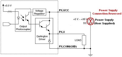
Figure 10: Damage Due to Reverse Power Supply Connections