NI USB-8451, Atmel AT25080A, and the LabVIEW SPI API
Overview
For the purposes of this tutorial, we are using the AT25080A as an example. This is a general purpose EEPROM which uses the SPI bus for communication.
To learn more about the SPI bus or the I2C bus, please see the Introduction to SPI and Introduction to I2C bus documents linked at the bottom of this Developer Zone document.
Contents
- Physical Connection
- Understanding Your Device’s Functionality
- Implementing an Example in LabVIEW with SPI Advanced API
- SPI Basic API
- Conclusion
- Related Links
Physical Connection
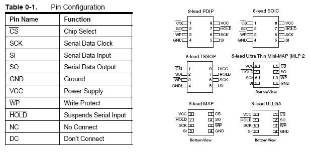
The first step is to look at the physical aspects of your device and the NI USB-8451. We can find the pinout in our device’s manual. Figure 1 and Figure 2 show the pinouts of the AT25080A and NI USB-8451. If you are interested in more information regarding the pinouts of the AT25080A or another SPI communicating device, refer to the product’s manual.
[+] Enlarge Image
Figure 1: AT25080A Pin Configuration from AT25080A Product Manual
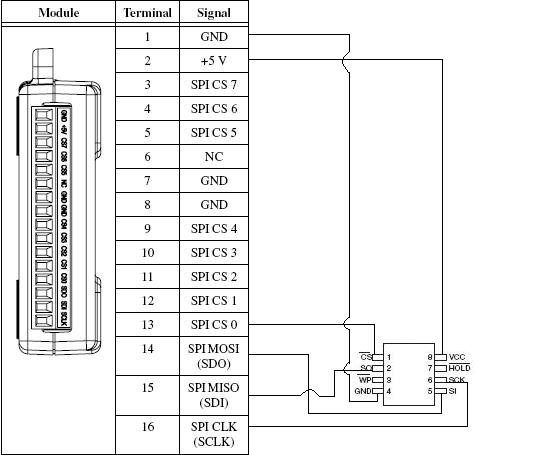
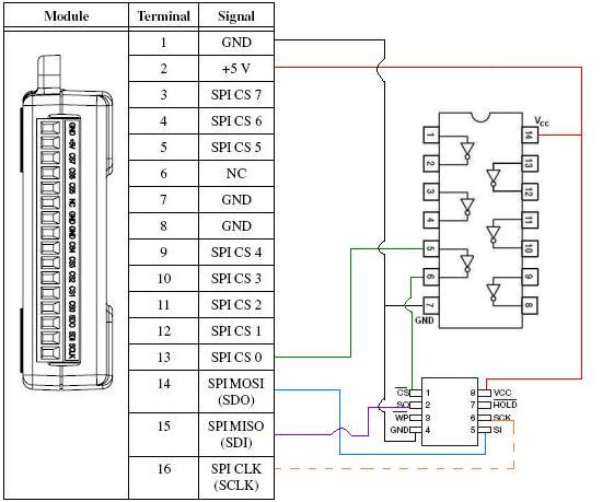
The next step is to connect the pins from our device to the NI USB-8451. Figure 2 shows how to connect the AT25080A and the NI USB-8451.
Figure 2: NI USB-8451 connection to AT25080A
Begin by connecting the 5 V supply (VCC) and ground (GND) to the AT25080A. You should verify that the USB-8451 can power your chip by looking at the power requirements sections of the chip’s manual. The USB-8451 can supply 230mA. In this case, this is enough to power the chip. The next step is to connect the clock signal. We can connect the Master Out Slave In (MOSI or SDO) pin from the NI USB-8451 to input of the integrated circuit. For the AT25080A, this pin is called Slave In (SI). In some cases, it may also be called MOSI. Another signal to connect is the Master In Slave Out (MISO or SDI) to the output of the chip. Again, this pin is named Slave Out for the AT25080A. The final pin to connect is the Chip Select (CS) signal. In this application we only have a single chip, so connect CS0 directly to the chip CS pin.
Please note that the chip select is active low, which means the chip enables communication when the signal is low and remains idle when the signal is high. This is the default behavior of the NI USB-8451, as well as the default for many devices on the market. If this is not the case for another device, please refer to the subsection “What if My Chip Select needs to be Active High?” at the end of this section.
Notice that there are two pins not connected in this case. The WP and HOLD pins are used for other functionality outside of SPI protocol. For example, the HOLD pin can be used to pause serial communication without resetting the serial sequence. The complete functionality is usually detailed in the user manual of that particular device. The way you connect these pins also depends on the functionality. Keep in mind that the USB-8451 also has digital IO lines that can be used for this kind of application.
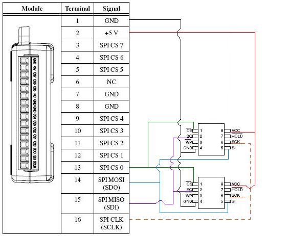
Figure 2 shows the connection diagram if you are using a single chip, however, one of the benefits of using the SPI communication bus is that it simplifies the connectivity and communication with many devices. An example is shown in Figure 3.
Figure 3: NI USB-8451 connection to multiple AT25080A devices
What if My Chip Select needs to be Active High?
If we are presented with this situation, we have two options to choose from. One method is to use LabVIEW to change the operation of chip selects to active high. NI provides a KnowledgeBase document that describes this method for the NI USB-8451:
KnowledgeBase 4ORH47OH: NI-8451 SPI Chip Select Active High
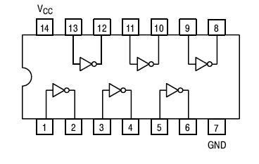
A second option is the use of another integrated circuit chip. For example, we can use a basic hex inverter as shown in Figure 4.
Figure 4: Basic Hex Inverter Chip
In this situation, we would provide a 5 V signal, ground (GND), and the chip select signal from the NI USB-8451. It is important to input the chip select signal from the NI USB-8451 to the input of an inverter on the hex inverter chip (e.g., pin 5) and then connect the output of the inverter to the chip select on the AT25080A (e.g., pin 6). This connection looks like Figure 5.
Figure 5: NI USB-8451, AT25080A, and Hex Inverter
Understanding Your Device’s Functionality
The previous section depicted how to set up for SPI communication between your NI USB-8451 and the AT25080A. Now we need to determine how to communicate to our device. The AT25080A is an EEPROM, so we want to write data to it and then read this data back. In this case, reading and writing are different operations for the device. If this was an Analog to Digital Converter, an operation could be to set the voltage output. We need a way to tell the device what operation we want to accomplish if we are writing or reading. This is done by using instructions.
When using the AT25080A, we can reference the product manual for the functional description of SPI programming. The product manual for this integrated circuit indicates the AT25080A uses an 8-bit instruction register. Figure 6 shows this instruction set. The instruction format is important to note as it indicates which instruction is being requested. Note that a “X” can be a 1 or 0.
Figure 6: Instruction Set for the AT25080A from AT25080A Product Manual
The instruction set shown in Figure 6 overviews three main features: the enable latch, the status register, and the memory array. Given these features, we can either set/reset or read/write to them. The instruction set shows us how to format the instruction when we want to perform that operation. In the following subsections, we discuss the timing and implementation for the READ, WREN, and WRITE instructions of the memory array.
Functional Descriptions for the WREN, WRITE, and READ Instructions
Referencing page seven of the AT25080A product manual, the most significant bit (MSB) is the first bit transmitted and received. It also mentions that once the AT25080A is selected with an active low chip select, the first byte is received thereafter. This byte is the op-code that defines the operations to be performed. In our case, this is a Read Data from Memory Array or Write Data to Memory Array operation. If we send an invalid op-code, no data is shifted into the AT25080A; data is not accepted via the SI pin, and the serial output pin (SO) remains in a high impedance state.
WREN (referenced from AT25080A product manual on page nine):
The device powers up in the write disable state when Vcc is applied. All programming instructions must therefore be preceded by a Write Enable instruction.
The timing diagram for the WREN instruction (Figure 7) shows the chip select going low, which indicates the AT25080A has been selected to receive information on the SI line. At that time the WREN op-code is delivered to the AT25080A and the SO line remains in a high impedance state. The chip select also returns to an idle state (high) when the operation is complete.
[+] Enlarge Image
Figure 7: Timing Diagram for WREN Instruction from AT25080A Product Manual
WRITE (referenced from AT25080A product manual on page eleven):
In order to program the AT25080A, two separate instructions must be executed. First, the device must be write enabled via the WREN instruction. Then a write (WRITE) instruction may be executed. Also, the address of the memory location(s) to be programmed must be outside the protected address field location selected by the block write protection level. During an internal write cycle, all commands are ignored except the RDSR instruction. For more information regarding the block write protection and protected address fields, refer to the AT25080A product manual.
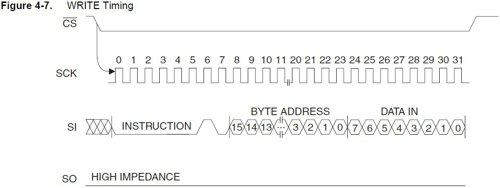
A write instruction requires the following sequence. After the chip select line is pulled low to select the device, the WRITE op-code is transmitted via the SI line followed by the byte address (A9-A0) and the data (D7-D0) to be programmed. Programming starts after the chip select pin is brought high. The low-to-high transition of the chip select pin must occur during the SCK low-time immediately after clocking in the D0 (LSB) data bit. The READY/BUSY status of the device can be determined by initiating a read status register (RDSR) instruction. If Bit 0 = “1”, the write cycle is still in progress. If Bit 0 = “0”, the write cycle has ended. Only the RDSR instruction is enabled during the write programming cycle. The AT25080A is capable of a 32-byte page write operation. After each byte of data is received, the five low-order address bits are internally incremented by one; the high-order bits of the address remain constant. If more than 32 bytes of data are transmitted, the address counter rolls over and the previously written data is overwritten. The AT25080A is automatically returned to the write disable state at the completion of a write cycle. For more information regarding the use of the status register, reference the AT25080A product manual.
NOTE: If the device is not write-enabled (WREN), the device ignores the write instruction and returns to the standby state when chip select is brought high. A new CS falling edge is required to reinitiate the serial communication.
Similarly to the READ timing, the chip select goes low and the SCK signal regulates the bits received on the SI line. The SO line remains in a high impedance state throughout the operation. Once in active low, the AT25080A receives the WRITE instruction followed by a byte address and the data to be to written. As with the other operations, the chip select finishes the operation by returning to an idle state (high).
[+] Enlarge Image
Figure 8: Timing Diagram for WRITE Instruction from AT25080A Product Manual
READ (referenced from AT25080A product manual on page eleven):
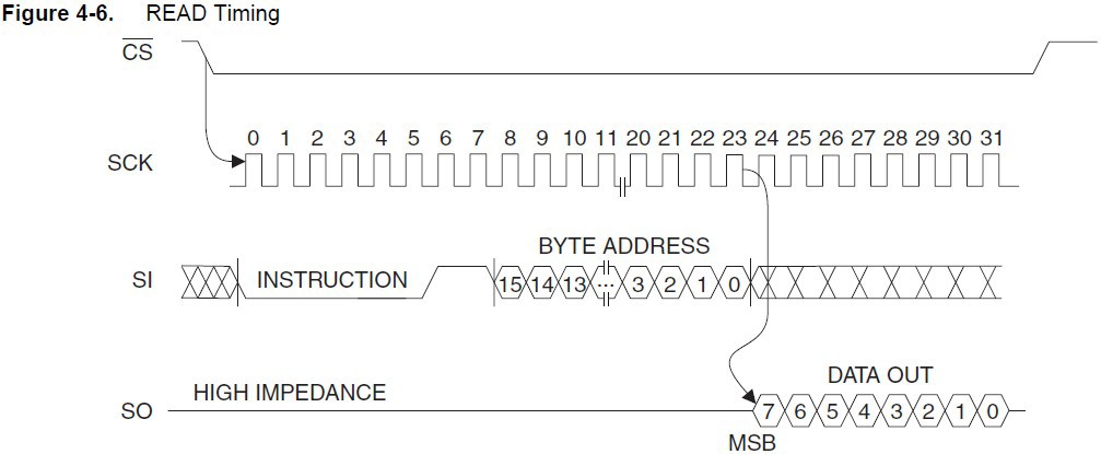
Reading the AT25080A via the Serial Output (SO) pin requires the following sequence. After the chip select line is pulled low to select a device, the READ op-code is transmitted via the SI line followed by the byte address to be read (A9-A0). Upon completion, any data on the SI line is ignored. The data (D7-D0) at the specified address is then shifted out onto the SO line. If only one byte is read, the CS line should be driven high after the data comes out. The read sequence can be continued since the byte address is automatically incremented and data continues to be shifted out. When the highest address is reached, the address counter rolls over to the lowest address allowing the entire memory to be read in one continuous read cycle.
In Figure 9, we can see the timing of the READ instruction. Notice how the chip select goes low and the SCK signal regulates the bits received and delivered on the SO and SI lines. In our case, the AT25080A sees the READ instruction followed by the byte address. The AT25080A then provides the data requested by the byte address as defined in the functional description. Note how the chip select returns to an idle state as it returns high.
[+] Enlarge Image
Figure 9: Timing Diagram for READ Instruction from AT25080A Product Manual
Implementing an Example in LabVIEW with SPI Advanced API
Implementing this process in LabVIEW is relatively straight forward. First we need to consider what we would like to do. Note that we are using the SPI Advanced API to create custom SPI transactions for our integrated circuit. This means that our first step is to create a script that describes the communication for our NI USB-8451 and the AT25080A (e.g., chosen chip select and instruction). Then we execute the script. SPI Advanced Vis can be found be right-clicking on the block diagram and navigating to Instrument I/O»NI-845x»SPI Advanced.
The first step when creating a custom SPI script is to set the clock polarity (CPOL) and phase (CPHA). Remember that CPOL and CPHA determine the clock idle state and the edge of the clock signal when the data on MISO or MOSI is driven or sampled. You can review this in the Overview of SPI tutorial linked at the bottom of this document. In our case, we need maintain convention such that data is read on the clock's rising edge and data is changed on the clock’s falling edge when reading, writing, etc. We are using 0 for CPOL and CPHA, but you could use 1 for CPOL and CPHA as well. This convention is shown in the timing diagram for the READ instruction, Figure 9.
Next we need to consider our SCK Clock Frequency (fsck). Referencing Figure 10, we can see the recommended clock frequencies given the voltage ranges. We are using 1000 Hz, which satisfies every range.
[+] Enlarge Image
Figure 10: Table of Applicable Frequencies for SCK from AT25080A Product Manual
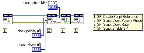
Now we have determined the beginning of each script we create in LabVIEW for our AT25080A. It includes a SPI Create Script Reference, SPI Script Clock Polarity Phase, and SPI Script Clock Rate with the settings we described above. These VIs are then followed by a SPI Script Enable SPI VI to switch the pins on an SPI port specified using NI-845x SPI Run Script.vi to master mode function. It also switches all chip select pins from tristate to push-pull output driven high. These VIs are shown in Figure 11.
Figure 11: Initial Script for any Instruction Sent to the AT25080A
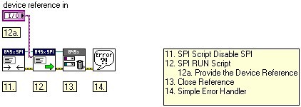
Following the SPI Script Enable SPI VI are the VIs that implement the instructions detailed by their timing diagrams. Once these VIs have been coded, we need to disable SPI and close our references, etc. This is typically done with the following VIs: SPI Script Disable SPI, SPI Run Script, Close Reference, and Simple Error Handler.
Figure 12: Series of VIs Used to Run and Close SPI Scripting
These VIs can also include an extra VI that is used when we try to read data in SPI. This VI is called SPI Extract Read Data. Figure 13 shows the added VI with a connection to an earlier SPI Script Write Read’s script read index output. This is covered in more detail in Scenario 3.
[+] Enlarge Image
Figure 13: Series of VIs Used to Run and Close SPI Scripting When Performing a Read
The following sections cover three scenarios that overview LabVIEW and the different instructions we have discussed above in detail.
Scenario 1: Set Write Enable Latch
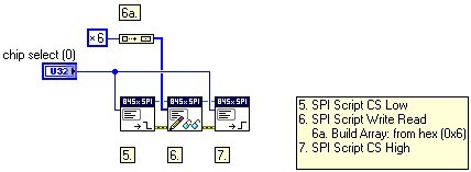
Referencing the timing diagram shown in Figure 7, we can see that we need to set the chip select low, provide the WREN hex instruction, and then reset the chip select high. As seen in Figure 7, the WREN instruction is 0000 X110 or 0x6 in hexadecimal representation. This process requires the use of three VIs: SPI Script CS Low, SPI Script Write Read, and SPI Script CS High.
Figure 14: Series of VIs to the Set Write Enable Latch Instruction
Scenario 2: Write Data to Memory Array
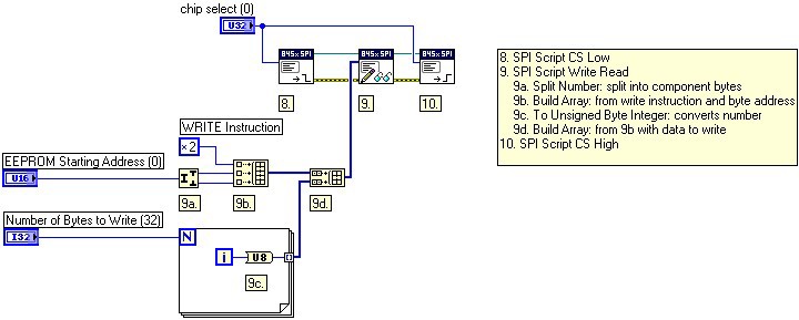
This scenario is a bit more advanced than the Set Write Enable Latch instruction. In order to write data to the memory array, we need to enable the Set Write Enable Latch. This causes us to use the same VIs in Figure 14, as well as those required to write data to the memory array. The timing diagram in Figure 8 shows the need to set the chip select low, provide the WRITE hex instruction and byte address, and then the data to be written. This process in a bit tricky, but let’s consider the VIs we need to implement this process: SPI Script CS Low, SPI Script Write Read, and SPI Script High.
[+] Enlarge Image
Figure 15: Series of VIs to Write Data to Memory Array
Other functions are also used to create mock data to be written to the memory array. In this case, we are using the EEPROM Starting Address, which is simply 0 unless we desire to write to a particular section of the memory array. Since we are using the AT25080A, we are only concerned with the addresses from A9-A0. On page twelve of the AT25080A product manual, addresses from A15-A10 are don't care bits. Don’t care bits can be any value. This leaves us with the data to be written. As stated in the functional description, we are able to write up to 32 bytes of data. We automatically create this by using a for loop and converting the iteration value to a byte and storing that value in a byte array. This byte array is then appended to the WRITE instruction and EEPROM starting address. This functionality is shown in Figure 15 (note: 9a, 9b, 9c, and 9d).
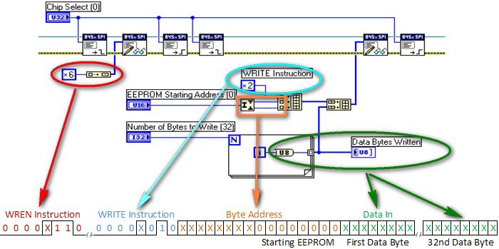
The entire process to write data to the memory array consists of two instructions. First, we have to input the WREN instruction to enable the write latch with an SPI Script Write Read VI. Next, we input the WRITE instruction with another SPI Script Write Read VI, followed by the byte address and data to be written. All of this interaction occurs on the SI line as shown in Figure 16.
[+] Enlarge Image
Figure 16: Overview of WRITE Instruction by Bits
Scenario 3: Read Data from Memory Array
This scenario is between the complexity levels of the WREN and WRITE instructions when implementing them in LabVIEW. The timing diagram for this instruction (Figure 9) sets the chip select low then provides the READ hex instruction followed by the byte address to read. The data is then presented on the MISO or (SO) line. Similar to the WRITE instruction, we use the following VIs: SPI Script CS Low, SPI Script Write Read, and SPI Script CS High.
[+] Enlarge Image
Figure 17: Series of VIs to Read Data from Memory Array
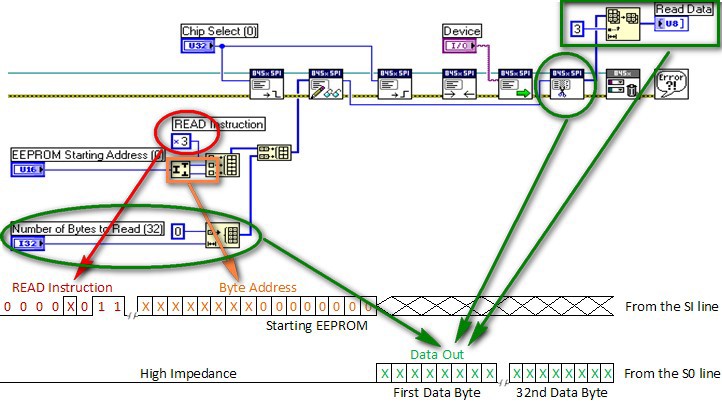
As we observed in Figure 16, we can overview the process of reading data from the memory array. This execution only requires one instruction. We start with the READ instruction and the byte address of the memory array as inputs to a SPI Script Write Read VI. This is the only information sent on the SI line. Finally, the data is outputted on the SO line with the help of a SPI Script Extract Read Data VI. This finishes the READ process as shown in Figure 18.
[+] Enlarge Image
Figure 18: Overview of READ Instruction by Bits
SPI Basic API
The Basic API is another option to communicate with your chip. The Basic API is useful if the operation of the chip involves user interaction. When using the SPI Advanced API, the user only sees all the data once the script has ended. This may be a limitation when using loops or benchmarking a program with timers—the user has to wait until the entire program has completed on the NI USB-8451 until they see the timers update or the see the data. This is overcome by using the Basic API, which does not run a script on the NI USB-8451, but sends command to the device to perform the operations. The downside is that sending these commands makes the Basic API less efficient. When performance is critical, it is highly advised to use the Script API.
Overview Basic API Programming for the AT25080A
Now that we are interested in using the Basic API to communicate with our AT25080A and NI USB-8451, let’s address the different programming steps. The first step when using the Basic API is to set the chip select, clock rate, clock polarity, and clock phase. This is done by using a NI-845x SPI Configuration node. Figure 19 shows this simple configuration, and this should appear at the beginning of any Basic API program.
[+] Enlarge Image
Figure 19: Initial Programming Steps for Basic API
Following the initial configuration, we can start programming our desired instruction. Let’s first consider the WREN instruction. In this case, we need to use a SPI Write Read VI and provide the correct hex instruction value (0x6). Figure 20 shows this functionality as programmed in LabVIEW with the Basic API.
Figure 20: Implementing the WREN Instruction in the Basic API
When we want to perform a WRITE instruction, we have to use the WREN instruction first. Next, we need to implement the WRITE instruction (hex 0x2). This is done similarly to the Advanced API, without the need to set and reset the chip select for the device. Figure 21 steps us through the Basic API and the idea of what is happening in this piece of code.
[+] Enlarge Image
Figure 21: Implementing the WRITE Instruction in the Basic API
If we want to create a program that reads the memory array with the Basic API, we need to use the same VIs in Figure 19 and the VIs in Figure 22 to implement the READ instruction. In this case we need to provide the READ instruction’s hex value of 0x3. This is very similar to the process performed in the Advanced API.
[+] Enlarge Image
Figure 22: Implementing the READ Instruction in the Basic API
The last step in the Basic API is to close the reference to the NI USB-8451. This is uses the same last two VIs as the Advanced API. These VIs are shown in Figure 23.
Figure 23: Closing a SPI program with the Basic API
Conclusion
Now we have covered the basic structuring of LabVIEW for SPI communication. It is now time for you to play with the AT25080A examples included with LabVIEW. To get to these examples, open LabVIEW and navigate to Help»Find Examples. In the Browse window, navigate to Hardware I/O»I2C and SPI»SPI Advanced or Hardware I/O»I2C and SPI»SPI Basic. If you have installed the NI-845x driver, you see two examples thoroughly discussed throughout this tutorial: Atmel AT25080A Read and Atmel AT25080A Write.
For more information regarding SPI programming refer to the related links.
